Monday, February 6th 2017

NVIDIA Unveils New Line of Quadro Pascal GPUs
NVIDIA today introduced a range of Quadro products, all based on its Pascal architecture, that transform desktop workstations into supercomputers with breakthrough capabilities for professional workflows across many industries. Workflows in design, engineering and other areas are evolving rapidly to meet the exponential growth in data size and complexity that comes with photorealism, virtual reality and deep learning technologies. To tap into these opportunities, the new NVIDIA Quadro Pascal-based lineup provides an enterprise-grade visual computing platform that streamlines design and simulation workflows with up to twice the performance of the previous generation, and ultra-fast memory.
"Professional workflows are now infused with artificial intelligence, virtual reality and photorealism, creating new challenges for our most demanding users," said Bob Pette, vice president of Professional Visualization at NVIDIA. "Our new Quadro lineup provides the graphics and compute performance required to address these challenges. And, by unifying compute and design, the Quadro GP100 transforms the average desktop workstation with the power of a supercomputer."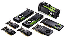 Benefits of Quadro Pascal Visual Computing Platform The new generation of Quadro Pascal-based GPUs -- the GP100, P4000, P2000, P1000, P600 and P400 -- enables millions of engineers, designers, researchers and artists to: -
"Professional workflows are now infused with artificial intelligence, virtual reality and photorealism, creating new challenges for our most demanding users," said Bob Pette, vice president of Professional Visualization at NVIDIA. "Our new Quadro lineup provides the graphics and compute performance required to address these challenges. And, by unifying compute and design, the Quadro GP100 transforms the average desktop workstation with the power of a supercomputer."

- Unify simulation, HPC, rendering and design - The GP100 combines unprecedented double precision performance(2) with 16GB of high-bandwidth memory (HBM2) so users can conduct simulations during the design process and gather realistic multiphysics simulations faster than ever before. Customers can combine two GP100 GPUs with NVLink technology and scale to 32GB of HBM2 to create a massive visual computing solution on a single workstation.
- Explore deep learning - The GP100 provides more than 20 TFLOPS of 16-bit floating point precision computing(3) -- making it an ideal development platform to enable deep learning in Windows and Linux environments.
- Incorporate VR into design and simulation workflows - The "VR Ready" Quadro GP100 and P4000 have the power to create detailed, lifelike, immersive environments. Larger, more complex designs can be experienced at scale.
- Reap the benefits of photorealistic design - Pascal-based Quadro GPUs can render photorealistic images more than 18 times faster than a CPU.
- Create expansive visual workspaces - Visualize data in high resolution and HDR color on up to four 5K displays.
- Build massive digital signage configurations cost effectively - Up to 32 4K displays can be configured through a single chassis by combining up to eight P4000 GPUs and two Quadro Sync II cards.
14 Comments on NVIDIA Unveils New Line of Quadro Pascal GPUs
That picture is nerdgasm stuff lol.
Though lo and behold, we have single slot designs! Something supposedly not achievable on consumer cards, even if they are half-height designs.
however, that bus width is not directly comparable with the one for gddr5(x) as hbm/hbm2 is not double- or quad-pumped like gddr5(x).
today, gddr5x solution is not that far behind and it becomes a question of tradeoffs, more than it should - cost vs primarily card real estate (and generally only minor boost to bandwidth). unfortunately i have not seen many details on cost of building hbm memory solution (and for completely logical reasons we probably never will) but as it includes interposer that is a large chip (albeit a simple one at a larger process node) it has to be considerably more expensive than traditional gddr5x pcb layout (that is almost the same as gddr pcb layouts have always been).
hynix documents have their current hbm2 handwidth spec at 205gb/s, gpus would include 2 or 4 of these stacks, amounting to ~400gb/s or ~800gb/s. current nvidia's 1080/titanx use gddr5x with 256/384-bit bus for 320gb/s and 480gb/s respectively.
this is a bit simplified of course. more pcb layers and larger pcb will help, with trace length becoming a problem at one point etc. naturally, this all adds to cost.
in case of hbm with its huge bus width, this is exactly what interposer is for. there is no need to run these traces on pcb from gpu to memory chips. instead, "traces" are from gpu to memory chips on the interposer.