News Posts matching #PLC

Return to Keyword Browsing

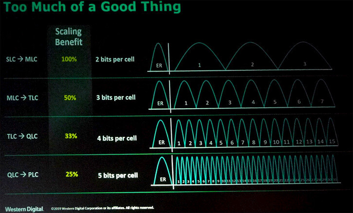
Server Shipment Growth and Spiking Pricing Push Total 2Q22 Enterprise SSD Revenue Growth to 31% QoQ, Says TrendForce

According to TrendForce research, material supply improvement and spiking demand for enterprise SSDs from North American hyperscale data center and enterprise clients in 2Q22 coupled with the Kioxia contamination incident in 1Q22 prompted customers to ramp up procurement to avoid future supply shortages. Manufacturers also give priority to meeting the needs of server customers due to the high pricing of enterprise SSD. In the second quarter, overall revenue of the enterprise SSD market increased by 31.3% to US$7.32 billion.

As the market leader, Samsung has grown its enterprise SSD revenue to US$3.26 billion with the recovery of enterprise SSD procurement. Especially in the second quarter, when orders for other consumer products continued to decline, enterprise SSD became the company's outlet for reducing production capacity. At present, Samsung has been continuously investing in the development of next-generation transmission specification products such as the CXL 2.0 product released at the Flash Summit in early August, in order to maintain a leading position in the market.

Western Digital May Introduce Penta Layer Cell (PLC) NAND by 2025

Western Digital has apparently delayed the introduction of Penta Layer Cell (PLC) NAND-based flash to 2025. The company had already disclosed development on the technology back in 2019, around the same time that Toshiba announced it (Toshiba which is now Kioxia, and a Western Digital partner in the development of the technology). The information was disclosed at Bank of America Merrill Lynch 2021 Global Technology Conference, where Western Digital's technology and strategy chief Siva Sivaram said that "I expect that transition [from QLC to PLC] will be slower. So maybe in the second half of this decade we are going to see some segments starting to get 5 bits per cell."

PLC is another density-increase step for NAND flash, whereby each NAND cell can have five bits written into it, thus increasing the amount of information available in the same NAND footprint. To achieve these 5 bits, each cell must store one of 32 voltage states, which in turn inform the flash controller of which corresponding data bits are stored herein. Siva Sivaram said that he expect the technology to take some more time to mature than most, due to the need for controller development that can take advantage of the increased density while making up for the shortcoming in this increased bit-per-cell approach (lower endurance and lower performance). PLC won't bring us HDD-tier storage density by itself (it only enables storage of 25% more data per cell); however, when paired with increasing layers of NAND flash, those 25% extra quickly add up.

Samsung Developing 160-layer 3D NAND Flash Memory

Samsung Electronics is reportedly developing its 7th generation V-NAND memory with ultra-high 3D stacking technology. The first model will feature at least 160 layers, subsequent models will feature more. In early signs of the company not wanting to yield the technological initiative to China's YMTC, the first 160-layer V-NAND by Samsung is slated to come out roughly around the time YMTC's 128-layer 3D NAND flash hits mass production, towards the end of 2020.

At the heart of the ultra-high 3D stack is Samsung's proprietary Double Stack technology. The double-stack technology creates electron holes at two separate times for current to go through circuits. The current-generation single-stack chips creates these holes once throughout the stack per cycle. The 160-layer NAND flash is expected to herald a 67% increase in densities per package over the 96-layer chips in the market. Densities could also be increased by other means such as switching to newer semiconductor fabrication nodes, and PLC (5 bits per cell), which is currently being developed by KIOXIA.

Samsung Introduces Industry's First All-in-One Power ICs Optimized for Wireless Earbuds

Samsung Electronics, a world leader in advanced semiconductor technology, today announced the industry's first all-in-one power management integrated circuits (PMIC), MUA01 and MUB01, optimized for today's True Wireless Stereo (TWS) devices.

Unlike wireless headphones, TWS earbuds have no wire that connects the two earpieces. Without the connecting wires, TWS devices present users with more freedom in movement and range on their day-to-day activities. However, like other mobile devices, long battery life and small form factors are key requirements for these wireless earbuds.
Samsung PMIC Samsung PMIC Samsung PMIC

Kioxia Develops New 3D Semicircular Flash Memory Cell Structure "Twin BiCS FLASH"

Kioxia Corporation today announced the development of the world's first three-dimensional (3D) semicircular split-gate flash memory cell structure "Twin BiCS FLASH" using specially designed semicircular Floating Gate (FG) cells. Twin BiCS FLASH achieves superior program slope and a larger program/erase window at a much smaller cell size compared to conventional circular Charge Trap (CT) cells. These attributes make this new cell design a promising candidate to surpass four bits per cell (QLC) for significantly higher memory density and fewer stacking layers. This technology was announced at the IEEE International Electron Devices Meeting (IEDM) held in San Francisco, CA on December 11th.

3D flash memory technology has achieved high bit density with low cost per bit by increasing the number of cell stacked layers as well as by implementing multilayer stack deposition and high aspect ratio etching. In recent years, as the number of cell layers exceeds 100, managing the trade-offs among etch profile control, size uniformity and productivity is becoming increasingly challenging. To overcome this problem, Kioxia developed a new semicircular cell design by splitting the gate electrode in the conventional circular cell to reduce cell size compared to the conventional circular cell, enabling higher-density memory at a lower number of cell layers.

Toshiba Talks About 5-Bit-per-Cell (PLC) Flash Memory

Toshiba at the Flash Memory Summit announced they've managed to develop a 5-Bit-per-Cell memory solution Based on its BiCS 4 flash memory technologies, the feat was achieved using a modified module of Quad-Level Cell (QLC) memory. This shows the technology is not only feasible, but has room for improvement, since an adapted QLC technology will always be inferior to a natively-developed, Penta-Level Cell (PLC) solution.

To achieve this ability to store one extra bit of information per cell (compared to QLC), a new level of voltage refinement is required: the cell has to be able to change its state according to one of 32 voltage states, which, in turn, have to be read out correctly by the flash memory controller. This reduces the cell's performance and endurance (as does any increase in the number of bits per cell), and will require a number of solutions to mitigate and compensate for this reduced performance. However, density has become an increasing concern from manufacturers, hence the continued development of deeper, more variable voltage states that allow for even more information to be stored in the same silicon area. Higher density means cheaper solutions, but density increased in such a way has known trade-offs that have been much talked about ever since the transition from Single-Level Cell (SLC) up to the (nowadays ubiquitous) QLC.
Return to Keyword Browsing
Apr 25th, 2024 14:16 EDT change timezone

New Forum Posts

Popular Reviews

Controversial News Posts