News Posts matching #Pyeongtaek

Return to Keyword Browsing

Samsung Semiconductor Discusses "Water Stress" & Impact of Production Expansion

"The Earth is Blue," said Yuri Gagarin, the first human to journey into space. With two-thirds of its surface covered in water, Earth is a planet that exuberates its blue radiance in the dark space. However, today, the scarcity of water is a challenge that planet Earth is confronted with. For some, this may be hard to understand. What happened to our blue planet Earth? To put in numbers, more than 97% of the water on Earth consists of seawater, with another 2% locked in ice caps. That only leaves a mere 1% of water available for our daily use. The problem lies in the fact that this 1% of water is gradually becoming scarcer due to reasons such as climate change, environmental pollution, and population growth, leading to increased water stress. 'Water stress' is quantified by the proportion of water demand to the available water resources on an annual basis, indicating the severity of water scarcity as the stress index rises. Higher stress indexes signify experiencing severe water scarcity.

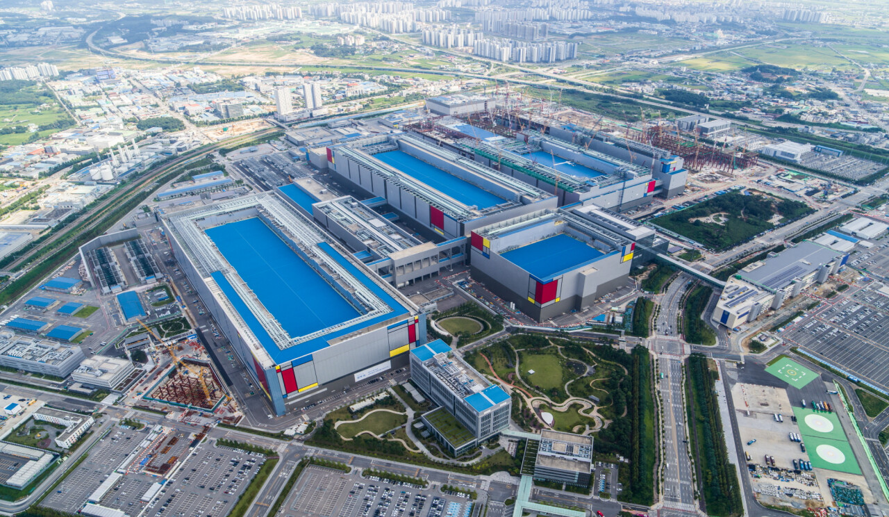
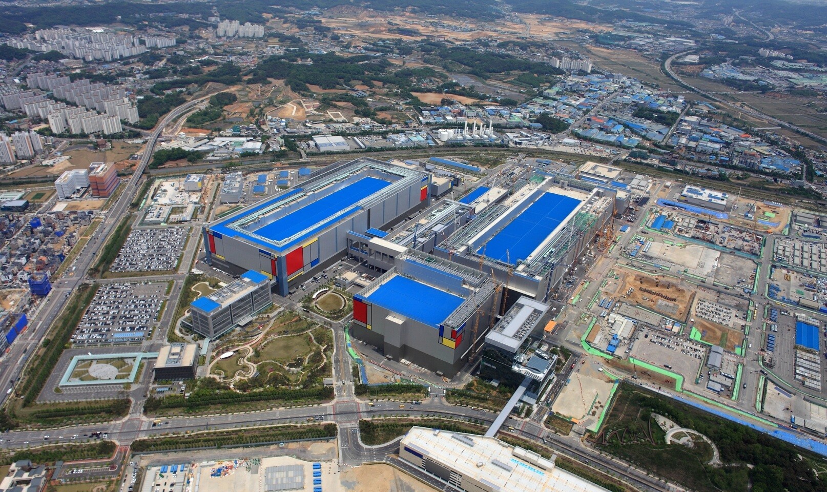
The semiconductor ecosystem, unsustainable without water
Because water stress issues transcend national boundaries, various stakeholders including international organizations and governments work to negotiate water resource management strategies and promote collaboration. UN designates March 22nd as an annual "World Water Day" to raise awareness about the severity of water scarcity running various campaigns. Now, it's imperative for companies to also take responsibility for the water resources given and pursue sustainable management.

Samsung Invested $37 Billion Expanding its Semiconductor Manufacturing Capacity in 2022

Samsung Electronics reportedly invested a record 53.11 trillion KRW (USD $40.2 billion) in expanding its semiconductor manufacturing capabilities, until March 2023, with investments throughout 2022 totaling $37 billion (47.87 trillion KRW). Business Korea reports that much of the investment was made toward increasing memory products manufacturing capacity, despite the ongoing slump in the PC and ICT industries from a possible economic recession. Samsung anticipates a continued growth in DRAM, possibly as the data-center and consumer-electronics industries transition to faster memory types. In particular, Samsung is undertaking a doubling in foundry capacity in its Pyeongtaek foundry.

Samsung Said to be Increasing Chip Production While Inflation is Increasing Cost of New Fabs

According to Reuters, Samsung is gearing up to increase the chip production capacity at its P3 factory in Pyeongtaek in South Korea, despite the fact that there's a general slowdown in the semiconductor industry, in addition to the general economic downturn. Samsung is apparently planning on adding 12-inch wafer capacity for DRAM, while also adding more 4 nm chip capacity. The P3 fab kicked off production of Samsung's most cutting-edge NAND flash chips earlier this year and is the company's largest fab overall. According to Reuters, Samsung is aiming to add at least 10 new EUV machines in 2023.

In related news via The Elec, Samsung has seen costs increase significantly when it comes to materials costs relating to the expansion of the P3 fab. So far, the company has racked up extra costs of over a trillion korean Won, or more than US$786 million, largely due to all of its contractors having raised their prices. The report also mentioned that some parts of the expansion of the P3 fab has been delayed by as much as a year, which isn't good news for Samsung and it likely means that the company will see further increases in costs before the expansions are finished.

Samsung Begins Mass Production of 16Gb LPDDR5 DRAM at World's Largest Semiconductor Line

Samsung Electronics, the world leader in advanced memory technology, today announced that its second production line in Pyeongtaek, Korea, has commenced mass production of the industry's first 16-gigabit (Gb) LPDDR5 mobile DRAM, using extreme ultraviolet (EUV) technology. Built on Samsung's third-generation 10 nm-class (1z) process, the new 16Gb LPDDR5 boasts the highest mobile memory performance and largest capacity to enable more consumers to enjoy the full benefits of 5G and AI features in next-generation smartphones.

"The 1z-based 16Gb LPDDR5 elevates the industry to a new threshold, overcoming a major developmental hurdle in DRAM scaling at advanced nodes," said Jung-bae Lee, executive vice president of DRAM Product & Technology at Samsung Electronics. "We will continue to expand our premium DRAM lineup and exceed customer demands, as we lead in growing the overall memory market."

DRAM Revenue Rises by 15.4% in 2Q20, with Possible Decline in Prices Expected for 3Q20, Says TrendForce

The last cyclical upturn in DRAM contract prices began at the start of 2020 and was led by server DRAM, according to TrendForce's latest investigations. In 2Q20, the emergence of the COVID-19 pandemic shocked the global economy, but OEMs maintained or even stepped up procurement of components because they feared disruptions in the supply chain. As a result, DRAM suppliers' bit shipments surpassed expectations for the quarter, in turn widening the overall increase in DRAM ASP and raising the global DRAM revenue by 15.4% QoQ in 2Q20 to US$17.1 billion.

Nevertheless, TrendForce indicates that server OEMs are now carrying a rather high level of DRAM inventory after aggressively stocking up for two consecutive quarters. At the same time, customers of enterprise servers are holding back on procurement because the economic outlook is getting bleaker and more uncertain. Since server DRAM has the unique role of leading cyclical changes, this category is going to be first to experience price drop in the next downturn and thereby pull prices down for other types of DRAM products. As such, TrendForce forecasts at best a flattening of product shipments and decrease in DRAM prices in 3Q20, with DRAM suppliers suffering a decline in profitability.

Samsung Electronics Announces Second Quarter 2020 Results

Samsung Electronics reported today KRW 52.97 trillion in consolidated revenue and KRW 8.15 trillion in operating profit for the second quarter ended June 30, 2020. Even as the spread of COVID-19 caused closures and slowdowns at stores and production sites around the world, the Company responded to challenges through its extensive global supply chain, while minimizing the impact of the pandemic by strengthening online sales channels and optimizing costs.

Quarterly operating profit rose 26 percent from the previous quarter and 23 percent from a year earlier, thanks to firm demand for memory chips and appliances, as well as a one-off gain at its Display Panel Business. A partial recovery in global demand since May also helped offset some COVID-19 effects, resulting in higher earnings than initially expected. Revenue in the quarter fell 4 percent from the previous quarter and 6 percent from a year earlier due to reduced sales of smartphones and other devices.

Samsung Receives Zero Waste to Landfill Validations for All of its Semiconductor Manufacturing Sites

Samsung Electronics Co., Ltd., a world leader in advanced semiconductor technology, today announced that it has received UL's Zero Waste to Landfill validation of Gold level and above for all of its global semiconductor operation sites. This signifies that Samsung's semiconductor sites in South Korea, US and China meet the requirement of more than 95-percent waste diversion through methods that do not involve thermal processing. In particular, the Samsung DSR building in Hwaseong, Korea, home to most of its local semiconductor R&D staff, is validated for Zero Waste to Landfill at the Platinum level for reaching 100-percent waste diversion.

"The Zero Waste to Landfill Gold validation is testament to the care and effort by our employees around the world to protect the environment," said Chanhoon Park, executive vice president of global infrastructure technology at Samsung Electronics. "Eco-friendly operations are now a must for any business and we will continue to ensure sustainable growth that is mindful of the environment that we live and operate in."

Samsung Expands its Foundry Capacity with A New Production Line in Pyeongtaek

Samsung Electronics Co., Ltd., a world leader in advanced semiconductor technology, today announced plans to boost its foundry capacity at the company's new production line in Pyeongtaek, Korea, to meet growing global demand for cutting-edge extreme ultraviolet (EUV) solutions.

The new foundry line, which will focus on EUV-based 5 nanometer (nm) and below process technology, has just commenced construction this month and is expected to be in full operation in the second half of 2021. It will play a pivotal role as Samsung aims to expand the use of state-of-the-art process technologies across a myriad of current and next generation applications, including 5G, high-performance computing (HPC) and artificial intelligence (AI).

Samsung Begins Mass-production of 512GB eUFS 3.1 Storage for Flagship Smartphones

Samsung Electronics, the world leader in advanced memory technology, today announced that it has begun mass producing the industry's first 512-gigabyte (GB) eUFS (embedded Universal Flash Storage) 3.1 for use in flagship smartphones. Delivering three times the write speed of the previous 512 GB eUFS 3.0 mobile memory, Samsung's new eUFS 3.1 breaks the 1 GB/s performance threshold in smartphone storage.

"With our introduction of the fastest mobile storage, smartphone users will no longer have to worry about the bottleneck they face with conventional storage cards," said Cheol Choi, executive vice president of Memory Sales & Marketing at Samsung Electronics. "The new eUFS 3.1 reflects our continuing commitment to supporting the rapidly increasing demands from global smartphone makers this year."
Samsung eUFS 3.1 512GB

Samsung Begins Mass Production of Industry's First 16GB LPDDR5 DRAM

Samsung Electronics, a world leader in advanced memory technology, today announced that it has begun mass producing the industry's first 16-gigabyte (GB) LPDDR5 mobile DRAM package for next-generation premium smartphones. Following mass production of the industry-first 12 GB LPDDR5 in July, 2019, the new 16 GB advancement will lead the premium mobile memory market with added capacity that enables enhanced 5G and AI features including graphic-rich gaming and smart photography.

"Samsung has been committed to bringing memory technologies to the cutting edge in allowing consumers to enjoy amazing experiences through their mobile devices. We are excited to stay true to that commitment with our new, top-of-the-line mobile solution for global device manufacturers," said Cheol Choi, senior vice president of memory sales & marketing, Samsung Electronics. "With the introduction of a new product lineup based on our next-generation process technology later this year, Samsung will be able to fully address future memory demands from global customers."

Samsung Begins Mass Production of Industry's First 12Gb LPDDR5 Mobile DRAM

Samsung Electronics, the world leader in advanced memory technology, today announced that it has begun mass producing the industry's first 12-gigabit ( Gb) LPDDR5 mobile DRAM, which has been optimized for enabling 5G and AI features in future smartphones. The new mobile memory comes just five months after announcing mass production of the 12 GB LPDDR4X, further reinforcing the company's premium memory lineup. Samsung also plans to start mass producing 12-gigabyte (GB) LPDDR5 packages later this month, each combining eight of the 12 Gb chips, in line with growing demand for higher smartphone performance and capacity from premium smartphone manufacturers.

"With mass production of the 12 Gb LPDDR5 built on Samsung's latest second-generation 10-nanometer (nm) class process, we are thrilled to be supporting the timely launch of 5G flagship smartphones for our customers worldwide," said Jung-bae Lee, executive vice president of DRAM Product & Technology, Samsung Electronics. "Samsung remains committed to rapidly introducing next-generation mobile memory technologies that deliver greater performance and higher capacity, as we continue to aggressively drive growth of the premium memory market."

Samsung Develops Industry's First 3rd-generation 10nm-Class DRAM

Samsung Electronics Co., Ltd., the world leader in advanced memory technology, today announced that it has developed a 3rd-generation 10-nanometer-class (1z-nm) eight-gigabit (Gb) Double Data Rate 4 (DDR4) DRAM for the first time in the industry. In just 16 months since it began mass producing the 2nd-generation 10nm-class (1y-nm) 8Gb DDR4, development of 1z-nm 8Gb DDR4 without the use of Extreme Ultra-Violet (EUV) processing has pushed the limits of DRAM scaling even further.

As 1z-nm becomes the industry's smallest memory process node, Samsung is now primed to respond to increasing market demands with its new DDR4 DRAM that has more than 20-percent higher manufacturing productivity compared to the previous 1y-nm version. Mass production of the 1z-nm 8Gb DDR4 will begin within the second half of this year to accommodate next-generation enterprise servers and high-end PCs expected to be launched in 2020.

Samsung Launches Industry's First 1TB Embedded Universal Flash Storage

Samsung Electronics, the world leader in advanced memory technology, today announced that it has begun mass producing the industry's first one-terabyte (TB) embedded Universal Flash Storage (eUFS) 2.1, for use in next-generation mobile applications. Just four years after introducing the first UFS solution, the 128-gigabyte (GB) eUFS, Samsung has passed the much-anticipated terabyte threshold in smartphone storage. Smartphone enthusiasts will soon be able to enjoy storage capacity comparable to a premium notebook PC, without having to pair their phones with additional memory cards.

"The 1 TB eUFS is expected to play a critical role in bringing a more notebook-like user experience to the next generation of mobile devices," said Cheol Choi, executive vice president of Memory Sales & Marketing at Samsung Electronics. "What's more, Samsung is committed to assuring the most reliable supply chain and adequate production quantities to support the timely launches of upcoming flagship smartphones in accelerating growth of the global mobile market."

Samsung Begins Mass Producing 2nd-Gen 10nm-Class, 16Gb LPDDR4X Mobile DRAM

Samsung Electronics, the world leader in advanced memory technology, today announced that it has begun mass producing the industry's first 2nd-generation of 10-nanometer-class (1y-nm), LPDDR4X (Low Power, Double Data Rate, 4X) DRAM to improve the efficiency and lower the battery drain of today's premium smartphones and other mobile applications. Compared to the mobile DRAM memory chips most used in current flagship mobile devices (1x-nm 16Gb LPDDR4X), the 2nd- generation LPDDR4X DRAM features up to a 10 percent power reduction while maintaining the same data rate of 4,266 megabits per second (Mb/s).

"The advent of 10nm-class mobile DRAM will enable significantly enhanced solutions for next-generation, flagship mobile devices that should first hit the market late this year or the first part of 2019." said Sewon Chun, senior vice president of Memory Sales & Marketing at Samsung Electronics. "We will continue to grow our premium DRAM lineup to lead the 'high-performance, high capacity, and low power' memory segment to meet the market demand and strengthen our business competitiveness."

Power Outage at Samsung NAND Flash Plant Cuts March Global Output by 3.5%

A power-outage on 9th March, at one of Samsung's NAND flash manufacturing plants located in Pyeongtaek, Korea, will have a notable impact on global NAND flash production. It reduced the global NAND flash output for the month of March 2018 by 3.5 percent, a number that isn't insignificant, and translates into non-volatile memory for millions of devices. It also trims Samsung's output by 11 percent for the month. SIlicon fabrication is a highly sensitive process, and the power-outage is said to have damaged up to 60,000 wafers of NAND flash chips.

The impact of this event on global prices of NAND flash memory, and devices based on it, remains to be seen. Any inflation could be nipped in the bud by Samsung and other NAND flash makers significantly increasing production through this quarter. Samsung will begin expansion of its NAND flash plant in Xi'an, China, which currently outputs 120,000 wafers per month, and is expected to put out 320,000 wafers a month after the expansion.

Samsung Electronics Breaks Ground on a New EUV Line

Samsung Electronics Co., Ltd., a world leader in advanced semiconductor technology, today broke ground on a new EUV (extreme ultraviolet) line in Hwaseong, Korea, aiming to maintain its leadership in state-of-the-art semiconductor technology. With this new EUV line, Samsung will be able to strengthen its leadership in the single nanometer process technology by responding to market demand from various applications, including mobile, server, network, and HPC (high performance computing), where high performance and power efficiency are critical.

The new facility is expected to be completed within the second half of 2019 and start production ramp-up in 2020. The initial investment in this new EUV line is projected to reach US$ 6 billion by 2020 and additional investment will be determined depending on market circumstances. Samsung has decided to utilize cutting-edge EUV technology starting with its 7-nanometer (nm) LPP (Low Power Plus) process. This new line will be set up with EUV lithography equipment to overcome nano-level technology limitations. Samsung has continued to invest in EUV R&D to support its global customers for developing next-generation chips based on this leading-edge technology.

Samsung to Invest $27.7 billion On Second Pyeongtaek Semiconductor Plant

Samsung's management committee has reportedly convened this morning, February 7th, to officially approve an investment plan on a new semicondctor manufacturing facility. Reports say this new factory is expected to be built on Pyeongtaek, the same general location as Samsung's current Pyeongtaek Fab 1. The investment plan is being made with plans for the plant to start production of the "P2-Project" plant during the first half of 2019.

Giving credence to these industry reports is the fact that Samsung has already celebrate gas pipeline contracts with companies (such as Wonik Holdings), just last month, in preparation for this new fab construction. It's as of yet unclear what specific plan the company has for the new factory, though it will certainly inject extraordinary new amounts of volume to Samsung's various foundry businesses. With two years of construction since it broke ground in May, 2015, the original fabrication line at the Pyeongtaek campus is currently the largest single Fab in the industry; in the face of this, it seems that a "first half of 2019" starting date for semiconductor production at Samsung's new manufacturing facilities may be slightly optimistic. However, those plans start to sound a little more on the doable side if one considers these might actually be plans for an expansion of the current Pyeongtaek Fab 1 facilities, plans for which the company has already announced back in July 2017.

Samsung Electronics to Increase its DRAM Output

Samsung Electronics, one of the largest manufacturers of DRAM and NAND flash memory, is poised to increase its production of DRAM. The company is bolstered by expansion of two of its DRAM manufacturing plants, located in Hwasung and Pyeongtaek, South Korea. The company is re-purposing a portion of its 2D NAND flash line at its Hwasung plant to produce DRAM. The new production line will begin its output from Q1-2018. The Pyeongtaek plant has been seeing similar activity where DRAM manufacturing clean-rooms are being built on the plant's second floor.

It's only in the second half of 2018 when end-users could expect Samsung's increased DRAM output to have any effect on prices of PC memory. The PC industry is not the only consumer of DRAM, as a larger share of it is consumed by the mobile industry (smartphones, tablets). DRAM inventories have been under tremendous strain over the past three quarters, which have forced PC memory prices to surge by 80-100 percent and beyond.

Samsung's New $13B V-NAND Factory Begins Production

Samsung is one of the top tech players in the world, with tendrils extending through almost all conceivable markets. That position, and the varied sources of income the company has at its disposal, gives it enough leeway to make investments that echo throughout the industry, Now, after a 15 trillion won investment (something like $13 billion), the company's latest V-NAND fab has started production in Pyeongtaek.

The fab will produce the firm's latest three-dimensional, 64-layer 256Gb V-NAND chips. Here's hoping the expected influx of higher quantities of NAND memory will allows us poor users to see a stop to the NAND pricing increase we've been seeing of late. Not everybody needs all the NAND available in smartphones.
Return to Keyword Browsing
Apr 24th, 2024 17:07 EDT change timezone

New Forum Posts

Popular Reviews

Controversial News Posts