Wednesday, February 25th 2026

Samsung is Transforming Old 2D NAND Fabs Into Modern HBM4 Production
Samsung is officially ending the production of its 2D NAND flash storage this year, and the company will be repurposing its old production lines to better fit the AI-driven demand. According to The Elec Korea, Samsung plans to officially stop 2D NAND production at its Hwaseong site, with Line 12 being the one carrying this aging technology. Instead of completely abandoning this facility, which houses plenty of chip-making tools, Samsung will repurpose them for DRAM metallization, which is the process of applying actual pathways within the DRAM itself to connect memory cells. Interestingly, the Hwaseong Line 12 holds a monthly wafer production capacity of 80,000 to 100,000 12-inch wafers. This is a significant number of wafers, which are now only used for 2D NAND Flash, a technology that is no longer needed in the wake of 3D NAND Flash technology.
Continuing the Line 12 legacy will be Samsung's 6th-generation 10 nm-class 1c DRAM, a technology used for HBM4, and Samsung expects the total wafer capacity for 1c DRAM to reach about 200,000 wafers per month in the second half of the year. Adapting the old 2D NAND Flash production site will definitely help, and Samsung will run this production along with Pyeongtaek Line 3 and Line 4.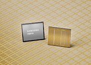
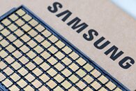 2D NAND Flash memory was first introduced in the late 1990s and has been in production since. Many memory and storage makers have been slowly phasing out this memory over the past few years, and Samsung is no different. In March, 2D NAND production will finally be stopped, making room for 3D NAND Flash technology that comes with many benefits over the old planar NAND, including higher capacities, better reliability, and much higher performance metrics across the board. One must bid farewell in order for the other to make room, meaning that with additional manufacturing capacity, Samsung could ease the storage shortage a bit.
Sources:
The Elec Korea, via Juakn05 on X
Continuing the Line 12 legacy will be Samsung's 6th-generation 10 nm-class 1c DRAM, a technology used for HBM4, and Samsung expects the total wafer capacity for 1c DRAM to reach about 200,000 wafers per month in the second half of the year. Adapting the old 2D NAND Flash production site will definitely help, and Samsung will run this production along with Pyeongtaek Line 3 and Line 4.


2 Comments on Samsung is Transforming Old 2D NAND Fabs Into Modern HBM4 Production