News Posts matching #RibbonFET

Return to Keyword Browsing

Intel Foundry Services (IFS) and Cadence Design Systems Expand Partnership on SoC Design

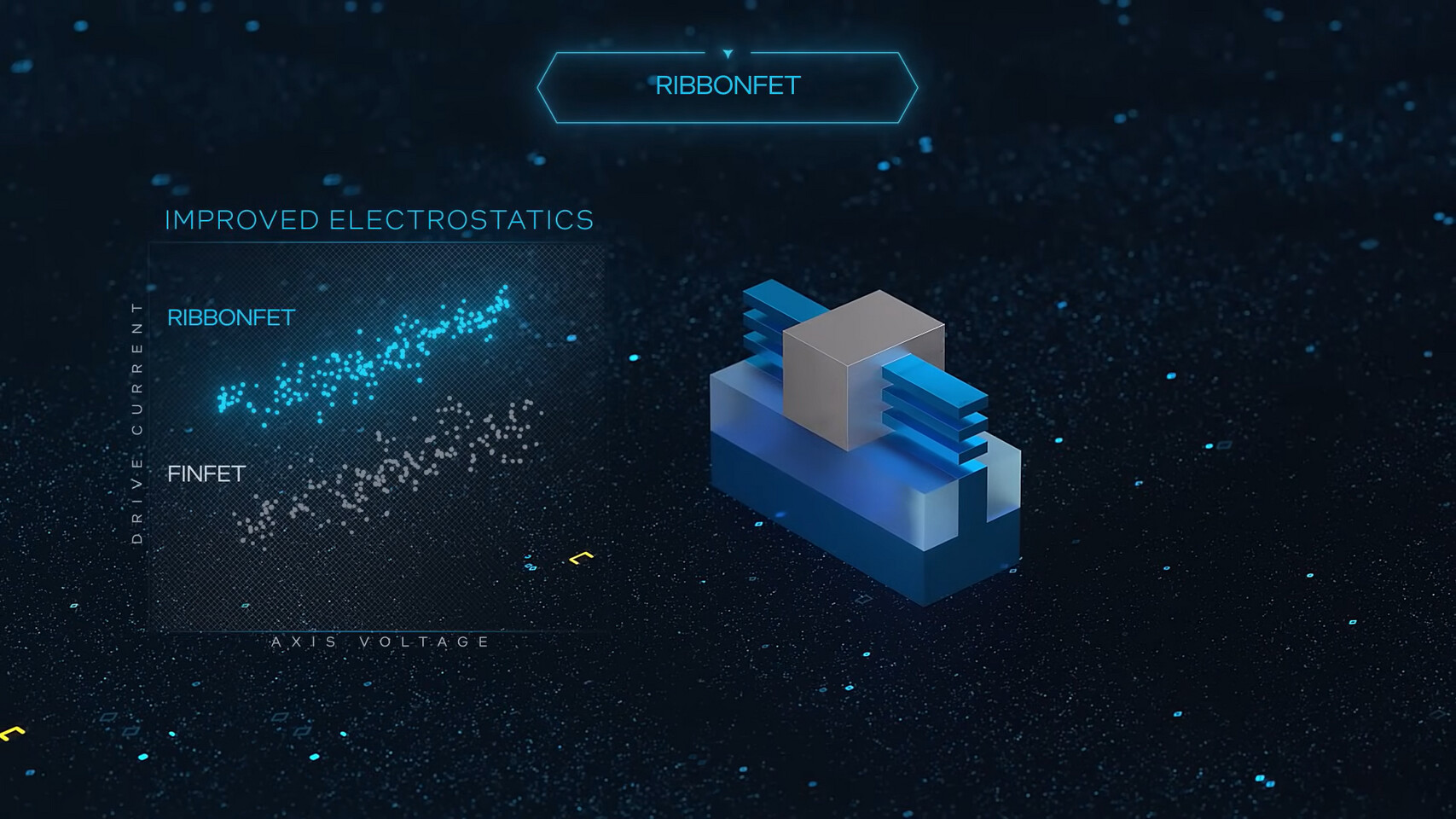
Intel Foundry Services (IFS) and Cadence Design Systems Inc. today announced a multiyear strategic agreement to jointly develop a portfolio of key customized intellectual property (IP), optimized design flows and techniques for Intel 18A process technology featuring RibbonFET gate-all-around transistors and PowerVia backside power delivery. Joint customers of the companies will be able to accelerate system-on-chip (SoC) project schedules on process nodes from Intel 18A and beyond while optimizing for performance, power, area, bandwidth and latency for demanding artificial intelligence, high performance computing and premium mobile applications.

"We're very excited to expand our partnership with Cadence to grow the IP ecosystem for IFS and provide choice for customers," said Stuart Paann, Intel senior vice president and general manager of IFS. "We will leverage Cadence's world-class portfolio of leading IP and advanced design solutions to enable our customers to deliver high-volume, high-performance and power-efficient SoCs on Intel's leading-edge process technologies."

Intel Demos 3D Transistors, RibbonFET, and PowerVia Technologies

During the 69th annual IEEE International Electron Devices Meeting (IEDM), Intel demonstrated some of its latest transistor design and manufacturing advancements. The first one in line is the 3D integration of transistors. According to Intel, the company has successfully stacked complementary field effect transistors (CFET) at a scaled gate pitch down to 60 nm. With CFETs promising thinner gate channels, the 3D stacked CFET would allow for higher density by going vertically and horizontally. Intel's 7 node has a 54 nm gate pitch, meaning CFETs are already close to matching production-ready nodes. With more time and development, we expect to see 3D stacked CFETs in the production runs in the coming years.

Next, Intel has demonstrated RibbonFET technology, a novel approach that is the first new transistor architecture since the introduction of FinFET in 2012. Using ribbon-shaped channels surrounded by the gate, these transistors allow for better control and higher drive current at all voltage levels. This allows faster transistor switching speeds, which later lead to higher frequency and performance. The width of these nanoribbon channels can be modulated depending on the application, where low-power mobile applications use less current, making the channels thinner, and high-performance applications require more current, making the channels wider. One stack of nanoribbons can achieve the same drive current as multiple fins found in FinFET but at a smaller footprint.

Intel's Arizona Expansion Marks Construction Milestone

Marking a milestone in Intel's ongoing manufacturing expansion in Arizona, the company today announced that the initial portion of the cleanroom is "weather tight" and the "blow down" phase has begun at the company's two new leading-edge chip factories on its Ocotillo campus in Chandler, Arizona. This milestone underscores Intel's dedication to advancing its presence in the state and fostering technological innovation.

"Our commitment to Arizona runs deep, and as we expand our operations, we remain dedicated to addressing the growing demand for semiconductors and helping the United States regain its leadership position in this vital industry. This milestone represents the result of great teamwork, proficient teams and exceptional craftsmanship of the tradespeople, and it's thanks to their hard work that we've made such significant progress on our site while keeping our culture of caring and the safety of all as our top priority." -Dan Doron, Intel vice president and general manager of Fab Construction Enterprise
Return to Keyword Browsing
May 16th, 2024 09:40 EDT change timezone

New Forum Posts

Popular Reviews

Controversial News Posts