News Posts matching #Tesla

Return to Keyword Browsing

Terafab Wants to Become One of the Largest Memory Makers by 2032

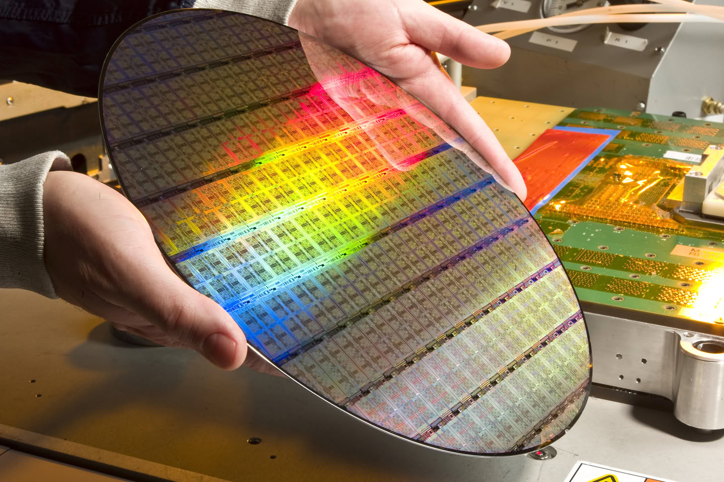
According to Nikkei, a procurement team from Terafab, the chip venture between Tesla and SpaceX, visited Japan and walked local equipment makers through what it plans to buy. The targets it reportedly shared are gigantic: 1 million wafers per month from 2032 onward, with around 700,000 of those going to memory chips and 300,000 to logic. Nikkei's headline puts that at 40 times the output of Japan's Rapidus. The same split first surfaced in a Jiji Press report last month, which said a single Texas plant would handle both memory and logic, with a pilot fab completed as early as July 2027. Intel is reportedly helping with logic using its 2 nm and 1.4 nm-class technology, while a Taiwanese company has been floated as a technology partner for memory. That could be Nanya, though nothing is confirmed.

For context, Samsung's entire DRAM output was estimated at 650,000 to 700,000 wafers a month late last year, while SK hynix was at about 550,000 earlier this year and hopes to reach roughly 1 million by 2030 or 2031. It isn't clear whether Terafab's memory figure covers DRAM alone or also includes NAND, so the Samsung comparison is a loose one. Musk has also been careful with his own dates. On an October SpaceX call, he put "big error bars" on reaching volume production by Q3 2028, with a first SRAM test chip planned for mid-2027 at Terafab's Austin research lab.
Samsung to Break Ground on Second Taylor Fab in November, Production Targeted for 2030

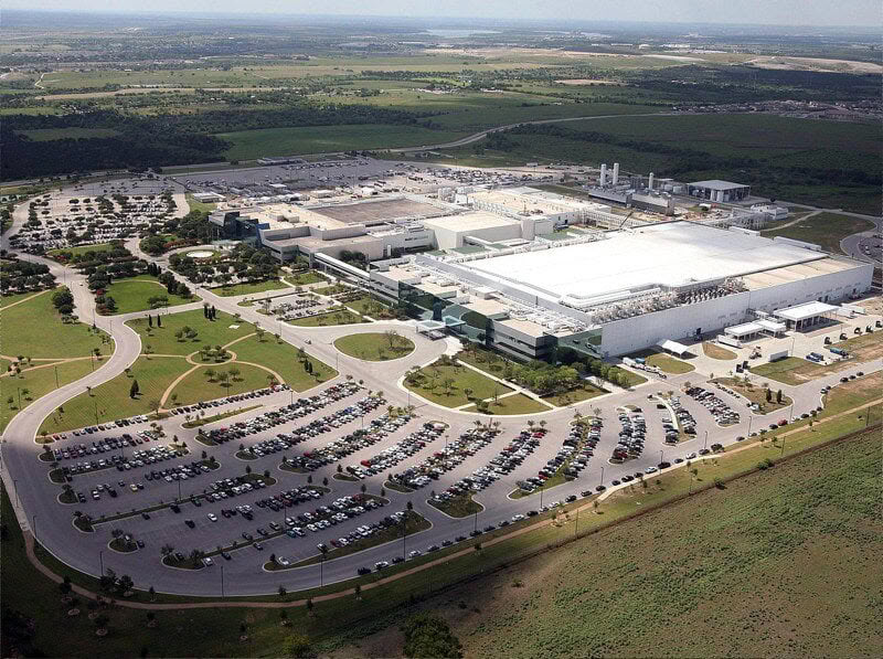
Samsung will reportedly break ground on its second chip fab in Taylor, Texas, this November, with mass production targeted for 2030. DigiTimes, citing South Korea's The Guru, reports that Taylor Fab 2 will span roughly 2.7 million square feet. Samsung also appears to have confirmed the timing at an October 15 event near the site, where Jonathan Taylor of Samsung Austin Semiconductor said construction should start early next month and that Fab 2 will be "one and a half times bigger than Fab One." In July, Samsung admitted that its leading-edge capacity was lagging customer demand, while inquiries for its 1.4 nm process, a node it was reportedly considering shelving last year, kept climbing. The process for Fab 2 hasn't been disclosed yet.

The first Taylor fab, which has slipped well past its original 2024 target, seems to be on track this time. Installed tools have started running processes as the plant goes through staged qualification. Fab 1 uses EUV lithography for Samsung's 2 nm process, with operations planned by the end of 2026 and volume production in 2027. Its best-known customer is Tesla, which signed a $16.5 billion deal running through 2033 that covers the AI6 chip, and Samsung is also set to build Tesla's AI5 on 2 nm in Texas. How orders will be split between the two fabs is unknown. Samsung plans to invest over $37 billion across Central Texas, backed by up to $4.745 billion in CHIPS Act funding. Given how long Fab 1 took, it's reasonable to expect that the 2030 target will depend heavily on demand.

Elon Musk's Terafab Faces Trademark Dispute Over Its Name

Tesla, SpaceX, and SpaceXAI have taken a trademark dispute over the "Terafab" name to federal court, PCMag reports. The declaratory judgment action was filed on September 15 in the US District Court for the Western District of Texas. It asks a judge to rule that Terafab does not infringe the "Tera-Fab" mark of Illinois nanotechnology firm Tera-print, which covers a desktop photolithography system used by researchers. Tera-print sent a cease-and-desist letter on May 23, days after Tesla filed its own Terafab trademark applications on May 18. Six settlement meetings between June and August apparently went nowhere, and Tera-print says it will defend its rights.

Nothing has been decided yet, and the claims are each side's own. Tesla and SpaceX point to a separate Tera-print application filed on May 22 that seeks coverage for semiconductor-related goods, and they call the timing opportunistic. That is their characterization, not a court finding. Tesla and SpaceX also argue the two operate in different product spheres and that confusion is unlikely. Musk announced Terafab in March as a chip factory for AI compute. Intel joined the project in April, though its exact role is unclear. Filings in May pointed to costs up to $119 billion across all phases, and in August the companies confirmed a Grimes County, Texas site with a $16.8 billion first phase.

Samsung Texas Fab to Mass-Produce Tesla AI5 SoC on 2 nm Node

Earlier this year, Elon Musk announced that Tesla had completed the design of its AI5 SoC. Today, we learn that the company will receive these processors from a United States-based Samsung fab located in Taylor, Texas. This means Samsung is preparing to produce the AI5 chip on its SF2 2 nm node on U.S. soil, effectively utilizing the CHIPS Act funding it received to manufacture silicon for domestic companies. As more companies push for domestic manufacturing, Tesla has been working with Samsung and TSMC to leverage their American-based facilities to align the vital parts of the supply chain with the location where the company is based and conducts most of its business.

For Samsung, this is a significant customer win, as Tesla will undertake major volume production in its Taylor fab on the SF2 node. This is one of the first major projects outside of Samsung's usual operations in South Korea, where most of its leading-edge production occurs. Regarding the AI5 chip, Tesla has designed these processors for Full Self-Driving (FSD). The CEO also mentioned that the AI5 chip will offer performance comparable to NVIDIA's "Hopper" architecture, with two AI5 units matching the power of a single "Blackwell" processor. On both the left and right sides, there are two rows of SK hynix LPDDR5X memory modules, each with three modules. This totals 12 LPDDR5X memory modules per AI5 chip. With 16 GB per module, this results in 192 GB of LPDDR5X memory per AI5 SoC. Additionally, Tesla has ambitious plans for nine-month design cycles for the AI6, which will also be part of the joint effort between Samsung, TSMC, and possibly even Intel with its advanced packaging. Musk confirmed that the AI6 and Dojo 3 projects, among other "exciting chips," are currently in progress, suggesting we could see much more custom silicon ASICs in the coming months.

Terafab's Cost Could Reach $119 Billion as First Phase Starts at $55 Billion

Elon Musk recently announced an ambitious project called Terafab, which he plans to build on Tesla's campus in eastern Travis County, Austin, Texas. Thanks to recent court hearings in Grimes County, Texas, we have learned that the first phase of the Terafab project is expected to cost $55 billion. However, if additional phases are constructed, this figure could rise to $119 billion. While this is an astonishingly high amount, it seems justified given Terafab's ambitious goals. Semiconductor manufacturing is one of the greatest marvels of the modern world, with only a few companies competing for the top spot. The engineering and scientific expertise required for building modern semiconductor manufacturing facilities is so rare that it is concentrated in just a few places around the globe.

The goal of Terafab is to consolidate the entire chip manufacturing process under one roof. The plant is expected to integrate several stages of semiconductor production at a single site, including logic fabrication, memory, packaging, testing, and mask production. This setup is unusual, as these steps are typically spread across multiple specialized facilities and companies. The idea behind Terafab is that consolidating these processes could accelerate development by allowing engineers to design, test, and revise chips with fewer delays, essentially enabling rapid prototyping. This contrasts with the traditional, lengthy process of manufacturing chips at one site, packaging them at another, and testing them in-house. A typical semiconductor fab for nodes below 3 nm costs over $20 billion, but that only covers silicon manufacturing. Terafab's goal to handle everything will push that cost astronomically high.

Tesla Tapes Out AI5 Chip in Partnership With TSMC and Samsung

Elon Musk announced today on X that Tesla has completed the design of a new generation of its AI chips for Full Self-Driving (FSD). The CEO also mentioned earlier that the AI5 chip will offer performance comparable to NVIDIA's "Hopper" architecture, with two AI5 units matching the power of a single "Blackwell" processor. In late 2025, reports indicated that Samsung had achieved a significant win for its previously struggling foundry business, as Tesla decided to split the manufacturing of its new AI5 accelerator between Samsung and TSMC. The chips will be produced at Samsung's plant in Taylor, Texas, and TSMC's facility in Arizona. This decision is part of a strategy to keep the supply chain diversified and maintain chip supply under control for any demand scenario.

Samsung and TSMC are not the only partners in this project. Tesla is also sourcing DRAM chips from SK hynix, which appear to be LPDDR5X memory integrated into the package. On both the left and right sides, there are two rows of SK hynix LPDDR5X memory modules, each with three modules. This totals 12 LPDDR5X memory modules per AI5 chip. With 16 GB per module, this results in 192 GB of LPDDR5X memory per single AI5 SoC.

Intel Joins Elon Musk's "Terafab" Project for Innovative Semiconductor Manufacturing

Intel has officially announced its participation in Elon Musk's "Terafab" project, which aims to reimagine chip manufacturing. Specifically, Intel Foundry plans to join this ambitious initiative, leveraging its significant manufacturing capabilities as one of the strategically important companies in the U.S. However, the specifics of Intel's involvement remain unclear, as it is not yet known how Intel will officially contribute to the Terafab project. The company has stated that since Terafab aims to produce 1 terawatt per year of compute power for AI and robots serving xAI, SpaceX, and Tesla. Intel will assist in designing silicon, manufacturing it, and providing some of the world's most advanced packaging technologies, such as EMIB. It is likely that some of Intel's facilities, which are currently being expanded, will become part of the network needed for the Terafab project, while the Terafab facility itself conducts custom work guided by Intel.

The goal of Terafab is to consolidate the entire chip manufacturing process under one roof. The plant is expected to integrate several stages of semiconductor production at a single site, including logic fabrication, memory, packaging, testing, and mask production. This setup is unusual, as these steps are typically spread across multiple specialized facilities and companies. The original idea behind Terafab is that consolidating these processes could accelerate development by enabling engineers to design, test, and revise chips with fewer delays, essentially allowing for rapid prototyping. This contrasts with the traditional, lengthy process of manufacturing chips at one site, packaging them at another, and testing them in-house. Elon Musk visited Intel's CEO Lip-Bu Tan over the past weekend securing a deal.

Elon Musk Prepares "TERAFAB" $20 Billion Semiconductor Manufacturing Plant

Semiconductor manufacturing is arguably one of the greatest marvels of the modern world, with only a few companies competing for the top spot. Recently, Elon Musk announced an ambitious project called "TERAFAB," which he plans to build on Tesla's campus in eastern Travis County, Austin, Texas. This initiative will be a joint effort involving Tesla, SpaceX, and xAI. Musk introduced this idea during a livestream on X as a practical solution to the growing gap between his companies' future chip needs and the current pace of global chip production. The project could become one of the most engineering-intensive tasks these companies have ever undertaken, with some estimates placing the capital expenditure at $20 billion.

As Tesla, SpaceX, and xAI require substantial computing power to support their expanding user base, relying solely on external suppliers is insufficient for the scale of growth Musk envisions. Tesla is known for utilizing TSMC, Samsung, and even some of Intel's manufacturing and packaging capabilities to support its chip production. However, with the creation of TERAFAB, these companies aim to gain more control over the entire chip development process. The plant is expected to integrate several stages of semiconductor production at one site, including logic fabrication, memory, packaging, testing, and mask production. This setup is unusual, as these steps are typically spread across multiple specialized facilities. Musk believes that consolidating these processes could accelerate development by enabling engineers to design, test, and revise chips with fewer delays.

Samsung Foundry Utilization Jumps to 80% This Quarter

Samsung Foundry has struck gold as its utilization rate has jumped to an impressive 80% this quarter. This comes after many years of struggling to achieve a good utilization rate, while competitors like TSMC have consistently led the adoption of newer nodes and gained a massive customer base. However, the situation has now changed, and Samsung's foundries are now operating at about 80% of total capacity, consistently producing silicon, with the Pyeongtaek Campus P2 and P3 leading the charge. Previously, these lines were only achieving a 50% booking rate last year and even struggled with insufficient production volume in the second half of 2024. Samsung uses these sites to manufacture 4 nm, 5 nm, and 7 nm nodes, which are now considered "mature," as the leading edge shifts to sub-3 nm production.

Part of the foundry revival is attributed to the strong demand for its 6th-generation HBM, coming in the form of HBM4 with a custom base die manufactured on the 4 nm node. While competitors are making HBM4 base dies on older nodes, Samsung is using a 4 nm custom base die that provides higher design density for any logic that ASIC makers want to implement. This can include some data processing that will aid the main accelerator in AI workloads. This has translated into high demand for Samsung Foundry products from external customers, who are now keeping production at high capacity.

Tesla Completes AI5 Chip, Revives Dojo 3 with Intel Packaging Deal

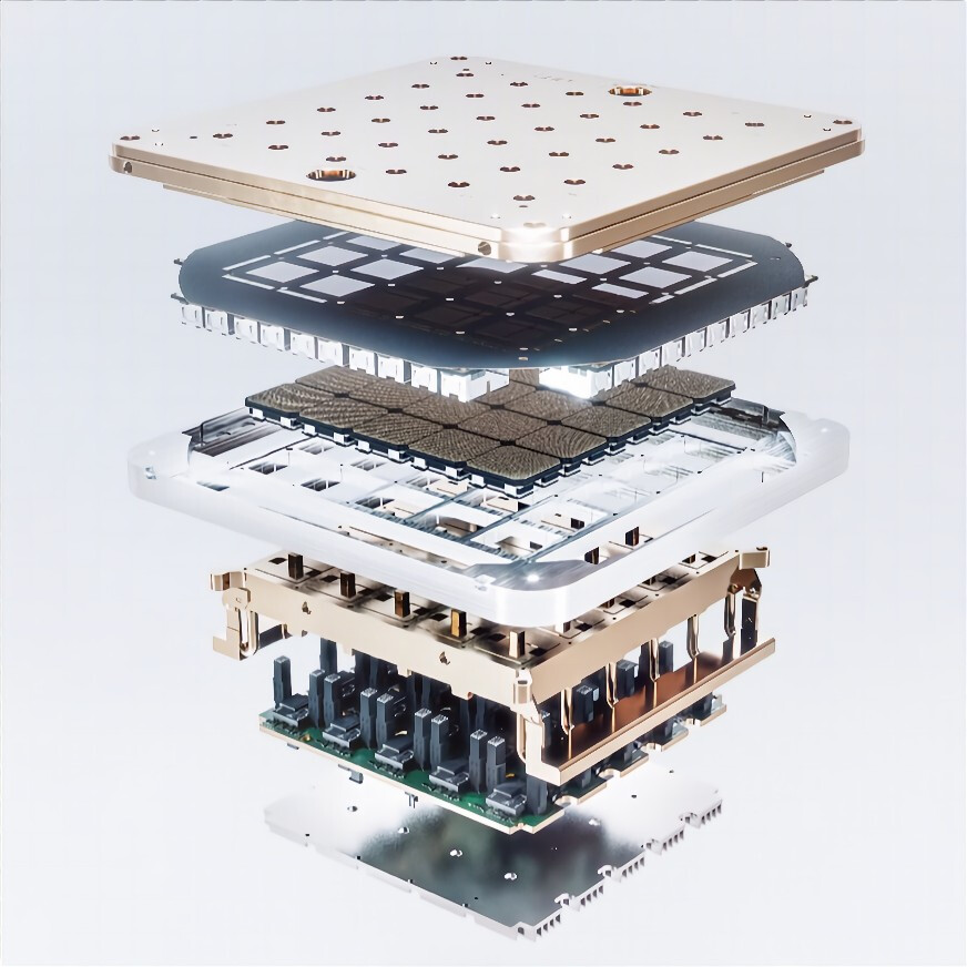
Tesla has finalized the development of its AI5 automotive processor, allowing for production at TSMC and Samsung facilities. This advancement also revives the previously halted Dojo 3 supercomputer project. CEO Elon Musk announced that the AI5 chip will offer performance on par with NVIDIA's "Hopper" architecture, with two AI5 units equaling the power of a single "Blackwell" processor. The revival of Dojo 3 project was rumored with Intel joining as a key packaging partner, marking a shift from Tesla's earlier dependence on TSMC for complete manufacturing. Intel will manage assembly and testing using its EMIB technology, which connects multiple dies via silicon bridges instead of a full-wafer interposer. This method is better suited to Tesla's large Dojo modules that combine several 654 mm² chips into a single package.

Also based on previous information, Samsung will produce the D3 training chips at its Texas facility using a 2 nm process, leaving Intel to oversee packaging operations exclusively. This division of labor addresses capacity constraints and provides Tesla with more flexibility in customizing interconnect layouts. For the AI5 automotive chips, both Samsung and TSMC will create distinct versions, but Tesla aims to ensure identical software performance across both. Initial projections suggest the AI5 could operate at just 150 W while matching the performance of NVIDIA's H100 accelerator that requires 700 W. This efficiency is achieved by removing general-purpose graphics subsystems and optimizing the architecture specifically for Tesla's neural processing.

NVIDIA to Build Seven New AI Supercomputers for U.S. Government

NVIDIA today announced that it is working with the U.S. Department of Energy's national labs and the nation's leading companies to build America's AI infrastructure to support scientific discovery, economic growth and power the next industrial revolution.

"We are at the dawn of the AI industrial revolution that will define the future of every industry and nation," said Jensen Huang, founder and CEO of NVIDIA. "It is imperative that America lead the race to the future—this is our generation's Apollo moment. The next wave of inventions, discoveries and progress will be determined by our nation's ability to scale AI infrastructure. Together with our partners, we are building the most advanced AI infrastructure ever created, ensuring that America has the foundation for a prosperous future, and that the world's AI runs on American innovation, openness and collaboration, for the benefit of all."

Samsung Foundry and TSMC Share Tesla AI5 Chip Production

Samsung has secured a significant win for its previously struggling foundry business as Tesla has decided to divide the manufacturing of its new AI5 accelerator between Samsung and TSMC. The chips will be produced at Samsung's plant in Taylor, Texas, and TSMC's facility in Arizona. This decision is part of a supply strategy following Samsung's previous $16.5 billion agreement to manufacture Tesla's upcoming AI6 processor. By using both top-tier foundries, Tesla aims to rapidly increase capacity while maintaining production within the United States. This dual-fab strategy is a pragmatic choice, allowing Tesla to avoid bottlenecks and build excess capacity for both its vehicles and expanding data-center needs. Elon Musk has praised Samsung's foundry capabilities, noting that the company already manages components of Tesla's AI4 platform, making the shared production of AI5 a logical step.

Meanwhile, Samsung is investing in next-generation High-NA EUV equipment and high-precision tools to close the gap with competitors on advanced nodes. The design of the AI5 chip is Tesla's desire for tight control of the componentry. Engineers have reportedly removed legacy GPU and image-signal blocks to create a more simplified chip optimized for real-time driving and AI workloads. This approach reduces die size and enhances cost efficiency. Tesla claims that the new architecture offers significantly better performance per dollar compared to its older designs, with company benchmarks indicating substantial improvements over AI4. In some cases, up to 40x performance improvements. Maybe the dream of Tesla Full Self-Driving (FSD) can now be accomplished with newer chips and better technology, if the conditions allow it.

Intel Wins Tesla Dojo 3 Packaging Contract in Dual-Supplier Strategy

Intel has secured Tesla as a customer for its specialized module-level packaging services, signaling that billions of investments and years of development are appealing to external Foundry Customers. Tesla's Dojo 3 initiative will see Samsung Electronics Foundry manufacture the custom D3 AI-training chips. At the same time, Intel handles the packaging and testing using its Embedded Multi-Die Interconnect Bridge (EMIB) technology, which connects multiple dies through silicon bridges rather than a full-wafer interposer. This dual-vendor approach diverges from Tesla's previous reliance on TSMC for both fabrication and System-on-Chip packaging. Tesla CEO Elon Musk confirmed that Samsung will focus on mass-producing the next-generation AI6 chips on a 2 nm process, and that the packaging will leverage Intel's EMIB platform.

Tesla's decision rests on the unique demands of its ultra-large Dojo modules, which pack multiple 654 mm² dies into a single array. Traditional packaging methods struggle to handle such sizes efficiently. TSMC's SoW solution faces capacity constraints amid high demand for CoWoS services. Intel's EMIB offers higher modularity, allowing Tesla to tailor interconnect layouts and integrate additional features as needed. Samsung's 2 nm node, paired with Intel's assembly expertise, provides Tesla with optimized yield, cost control, and a faster ramp-up for its AI infrastructure. This collaboration between two historic rivals is unusual, but much needed for both foundries to survive TSMC's competition. By splitting fabrication and packaging, Tesla aims to accelerate production for its full-self-driving systems, robotics ventures, and data-center operations.

Tesla Signs Massive $16.5 Billion Chip Supply Deal with Samsung Electronics

Tesla has entered a high volume chip supply agreement with Samsung Electronics valued at $16.5 billion, a deal seen by market observers as crucial to the fortunes of the Korean chip giant, which has been a loss-making business for the Samsung group. The deal will see Samsung supply Tesla's A16 and A15 SoCs for the various electronics of Tesla products. Leading this order will be Samsung's Taylor TX fab, which was built in assistance with the US CHIPS and Science Act, and took a $17 billion initial investment from the Samsung group. The fab broke ground in 2022.

The deal will see Tesla work closely with Samsung to optimize its manufacturing processes, ensuring that Tesla has greater control over the reliability of its chip supply, and there are no gotchas resulting from chip yields that could affect Tesla. In a post on X, Elon Musk said "Samsung agreed to allow Tesla to assist in maximizing manufacturing efficiency. This is a critical point, as I will walk the line personally to accelerate the pace of progress. And the fab is conveniently located not far from my house." Mass-production of Tesla SoCs from the Samsung Taylor Texas fab is expected to commence in late-2026. Commenting on this deal, Lee Dong-ju, an analyst at SK Securities, expects production in 2027 or 2028. Tesla sources its SoCs from both Samsung and TSMC, with the latter producing some of its SoCs in its Arizona fab.
TOP500: Frontier Keeps Top Spot, Aurora Officially Becomes the Second Exascale Machine

The 63rd edition of the TOP500 reveals that Frontier has once again claimed the top spot, despite no longer being the only exascale machine on the list. Additionally, a new system has found its way into the Top 10.
The Frontier system at Oak Ridge National Laboratory in Tennessee, USA remains the most powerful system on the list with an HPL score of 1.206 EFlop/s. The system has a total of 8,699,904 combined CPU and GPU cores, an HPE Cray EX architecture that combines 3rd Gen AMD EPYC CPUs optimized for HPC and AI with AMD Instinct MI250X accelerators, and it relies on Cray's Slingshot 11 network for data transfer. On top of that, this machine has an impressive power efficiency rating of 52.93 GFlops/Watt - putting Frontier at the No. 13 spot on the GREEN500.

Global Server Shipments Expected to Increase by 2.05% in 2024, with AI Servers Accounting For Around 12.1%

TrendForce underscores that the primary momentum for server shipments this year remains with American CSPs. However, due to persistently high inflation and elevated corporate financing costs curtailing capital expenditures, overall demand has not yet returned to pre-pandemic growth levels. Global server shipments are estimated to reach approximately. 13.654 million units in 2024, an increase of about 2.05% YoY. Meanwhile, the market continues to focus on the deployment of AI servers, with their shipment share estimated at around 12.1%.

Foxconn is expected to see the highest growth rate, with an estimated annual increase of about 5-7%. This growth includes significant orders such as Dell's 16G platform, AWS Graviton 3 and 4, Google Genoa, and Microsoft Gen9. In terms of AI server orders, Foxconn has made notable inroads with Oracle and has also secured some AWS ASIC orders.

Intel Should be Leading the AI Hardware Market: Pat Gelsinger on NVIDIA Getting "Extraordinarily Lucky"

Intel CEO Pat Gelsinger considers NVIDIA "extraordinarily lucky" to be leading the AI hardware industry. In a recent public discussion with the students of MIT's engineering school to discuss the state of the semiconductor industry, Gelsinger said that Intel should be the one to be leading AI, but instead NVIDIA got lucky. We respectfully disagree. What Gelsinger glosses over with this train of thought is how NVIDIA got here. What NVIDIA has in 2023 is the distinction of being one of the hottest tech stocks behind Apple, the highest market share in a crucial hardware resource driving the AI revolution, and of course the little things, like market leadership over the gaming GPU market. What it doesn't have, is access to the x86 processor IP.

NVIDIA has, for long, aspired to be a CPU company, right from its rumored attempt to merge with AMD in the early/mid 2000s, to its stint with smartphone application processors with Tegra, an assortment of Arm-based products along the way, and most recently, its spectacularly unsuccessful attempt to acquire Arm from Softbank. Despite limited luck with the CPU industry, to level up to Intel, AMD, or even Qualcomm and MediaTek; NVIDIA never lost sight of its goal to be a compute hardware superpower, which is why, in our opinion, it owns the AI hardware market. NVIDIA isn't lucky, it spent 16 years getting here.

Tesla Reportedly Doubling Dojo D1 Supercomputer Chip Orders

Tesla first revealed plans for its Dojo D1 training chip back in 2021, with hopes of it powering self-driving technology in the near future. The automative division has relied mostly on NVIDIA over the ensuing years, but is seemingly keen to move onto proprietary solutions. Media reports from two years ago suggest that 5760 NVIDIA A100 GPUs were in play to develop Tesla's advanced driver-assistance system (Autopilot ADAS). Tom's Hardware believed that a $300 Million AI supercomputer cluster—comprised of roughly 10,000 NVIDIA H100 GPUs—was powered on last month. Recent reports emerging from Taiwan suggest that Tesla is doubling Dojo D1 supercomputer chip orders with TSMC.

An Economic Daily report posits that 10,000 Dojo D1 are in a production queue for the next year, with insiders believing that Tesla is quietly expressing confidence in its custom application-specific integrated circuit (ASIC). An upcoming order count could increase for the next batch (in 2025). The article hints that TSMC's "HPC-related order momentum has increased thanks to Tesla." Both organizations have not publicly commented on these developments, but insider sources have disclosed some technical details—most notably that the finalized Dojo design: "mainly uses TSMC's 7 nm family process and combines it with InFO-level system-on-wafer (SoW) advanced packaging."

IBM Introduces its Granite Foundation Model

It's an exciting time in AI for business. As we apply the technology more widely across areas ranging from customer service to HR to code modernization, artificial intelligence (AI) is helping increasing numbers of us work smarter, not harder. And as we are just at the start of the AI for business revolution, the potential for improving productivity and creativity is vast. But AI today is an incredibly dynamic field, and AI platforms must reflect that dynamism, incorporating the latest advances to meet the demands of today and tomorrow. This is why we at IBM continue to add powerful new capabilities to IBM watsonx, our data and AI platform for business.

We have announced our latest addition: a new family of IBM-built foundation models which will be available in watsonx.ai, our studio for generative AI, foundation models and machine learning. Collectively named "Granite," these multi-size foundation models apply generative AI to both language and code. And just as granite is a strong, multipurpose material with many uses in construction and manufacturing, so we at IBM believe these Granite models will deliver enduring value to your business. But now let's take a look under the hood and explain a little about how we built them, and how they will help you take AI to the next level in your business.

Tesla Starts Building "First of its Kind" Data Center

According to the job listing found by Electrek, Tesla is currently hiring staff for Tesla's "1st of its kind Data Centers." Tesla is a company with a huge demand for computing, especially with training self-driving technology on its hardware. The company is building its training chips called Dojo D1, which is used to train neural networks that power the company's Full Self Driving (FSD) that is inferenced locally on each Tesla vehicle. However, to support such training infrastructure and other data processing, the company is in need of its own data centers, and the recruitment for it has just started.

It is interesting to mention a "first of its kind" data center, meaning that some unique design and/or application goal will be present. The global data center is roughly a 250 billion USD market, and with Tesla entering, we are still waiting to see the size of its investment. Nonetheless, the latest position, "Engineering Program Manager, Data Centers," will oversee these efforts and lead the end-to-end design and engineering of this supposedly unique data center.

ORNL's Exaflop Machine Frontier Keeps Top Spot, New Competitor Leonardo Breaks the Top10 List

The 60th edition of the TOP500 reveals that the Frontier system is still the only true exascale machine on the list.

With an HPL score of 1.102 EFlop/s, the Frontier machine at Oak Ridge National Laboratory (ORNL) did not improve upon the score it reached on the June 2022 list. That said, Frontier's near-tripling of the HPL score received by second-place winner is still a major victory for computer science. On top of that, Frontier demonstrated a score of 7.94 EFlop/s on the HPL-MxP benchmark, which measures performance for mixed-precision calculation. Frontier is based on the HPE Cray EX235a architecture and it relies on AMD EPYC 64C 2 GHz processor. The system has 8,730,112 cores and a power efficiency rating of 52.23 gigaflops/watt. It also relies on gigabit ethernet for data transfer.

Elon Musk Places Twitter Acquisition on Hold as Doubts Emerge Over its Userbase Data

Elon Musk in a late-Thursday tweet announced that he is placing his Twitter acquisition bid on "temporary hold" over doubts about the platform's spam-bot data. Twitter, in a recent SEC regulatory filing, disclosed that spam bots made up less than 5% of its userbase. The filing revealed that Twitter has 229 million users that viewed consistent ads, while fewer than 5% of the "monetizable daily active users" were fake or spam-bot accounts. Financial analysts predict the substantial fall in cryprocurrency values, as well as a $400 billion drop in market-capitalization of the Tesla stock since Musk announced plans to buy Twitter, may have made the world's richest man squeamish about buying Twitter, and that he is probably looking for a legally safe escape route from the deal. Twitter shares plummeted in value since the Musk tweet.

Tesla to Patch 130,000 Cars with AMD Ryzen APUs Due to Overheating

One of the electric vehicle driving forces in the car market, Tesla, has today announced that the company would have to issue a soft recall of a few select car models over an issue with overheating. The affected vehicles are Tesla Model 3 2022, Tesla Model S 2021-2022, Tesla Model X 2021-2022, and Tesla Model Y 2022. Tesla's infotainment system is powered by AMD Ryzen APUs, replacing the Intel Atom CPUs found in the previous models. With Ryzen APUs overheating, the infotainment system can lag or restart and sometimes cause it to get completely turned off. The problem is that the car's liquid cooling will prioritize cooling the batteries instead of the processor, causing it to overheat. Tesla issued a soft recall on these models, meaning that a regular firmware update will fix this issue.
TeslaTesla, Inc. (Tesla) is recalling certain 2021-2022 Model S, Model X, and 2022 Model 3 and Model Y vehicles operating certain firmware releases. The infotainment central processing unit (CPU) may overheat during the preparation or process of fast-charging, causing the CPU to lag or restart. A lagging or restarting CPU may prevent the center screen from displaying the rearview camera image, gear selection, windshield visibility control settings, and warning lights, increasing the risk of a crash. Tesla will perform an over-the-air (OTA) software update that will improve CPU temperature management, free of charge. Owner notification letters are expected to be mailed July 1, 2022. Owners may contact Tesla customer service at 1-877-798-3752. Tesla's number for this recall is SB-22-00-009.

Elon Musk Teases Steam Game Support for Tesla Infotainment System

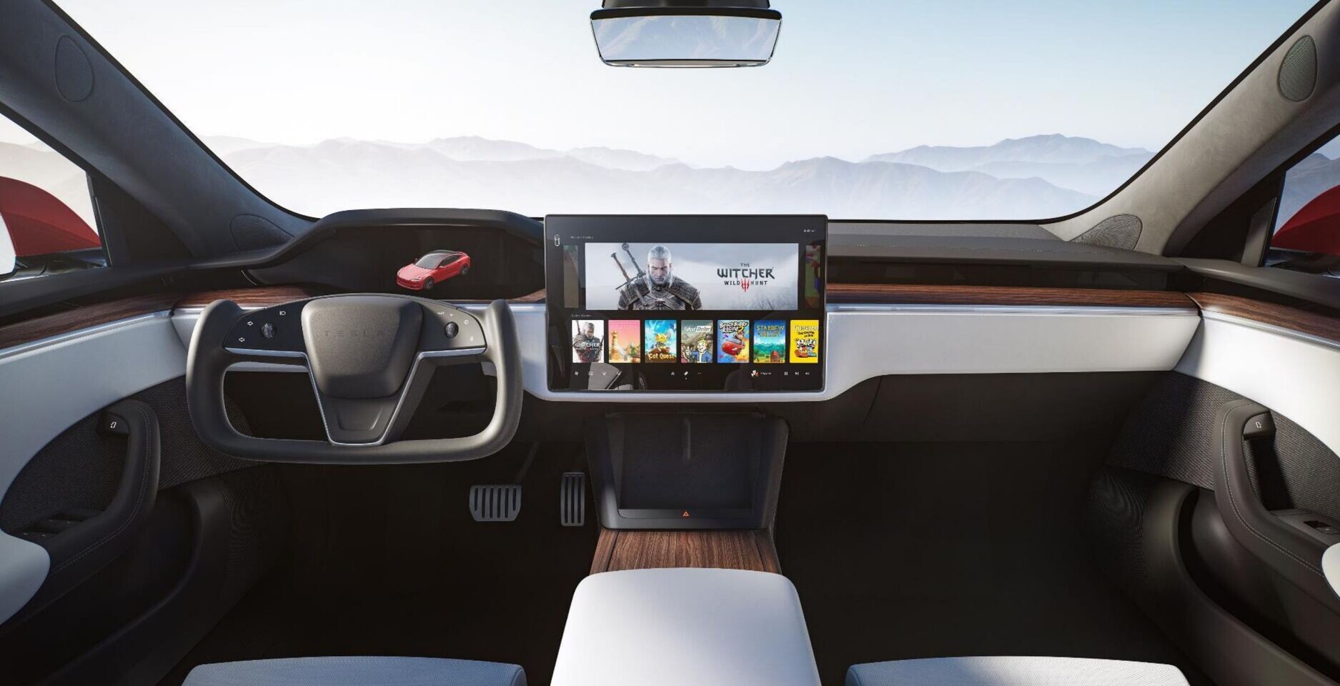
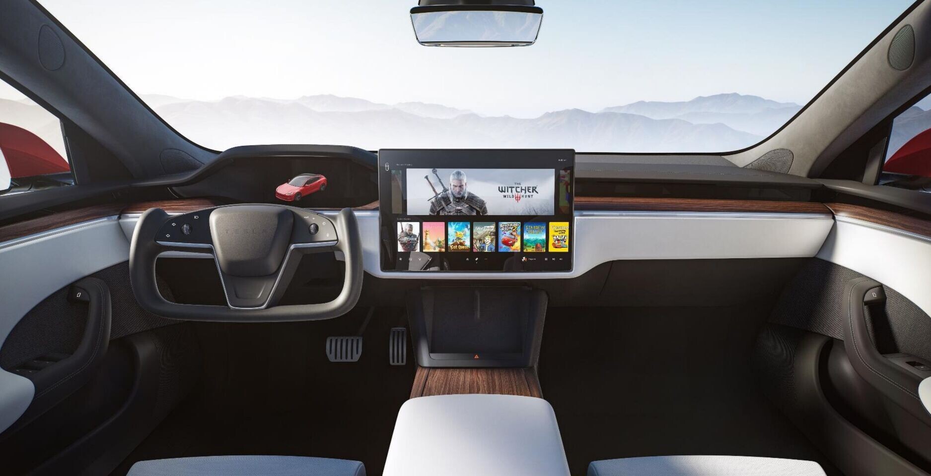
Tesla CEO Elon Musk has recently stated that Tesla is currently working on adding support for Steam games to the Linux-powered infotainment system found in Tesla cars. The latest hardware version of the Tesla infotainment system features a quad-core AMD Zen+ CPU paired with an Radeon Navi 23 GPU similar to that of the Xbox Series X/S, PlayStation 5, and Steam Deck. The GPU includes 28 Compute Units running at 2.8 GHz to drive the 17-inch 2200x1300 center screen for approximately 10 TFLOPS of performance. Tesla has previously worked to bring individual games to the infotainment system such as Beach Buggy Racing 2, The Battle of Polytopia, Cuphead, Stardew Valley, and Fallout Shelter in addition to the Atari 2600 emulator. The timeline for any such implementation is likely to be in the medium to long term.
Elon MuskWe're working through the general case of making Steam games work on a Tesla vs specific titles. Former is obviously where we should be long-term.

NVIDIA Unlocks GPU System Processor (GSP) for Improved System Performance

In 2016, NVIDIA announced that the company is working on replacing its Fast Logic Controller processor codenamed Falcon with a new GPU System Processor (GSP) solution based on RISC-V Instruction Set Architecture (ISA). This novel RISC-V processor is codenamed NV-RISCV and has been used as GPU's controller core, coordinating everything in the massive pool of GPU cores. Today, NVIDIA has decided to open this NV-RISCV CPU to a broader spectrum of applications starting with 510.39 drivers. According to the NVIDIA documents, this is only available in the select GPUs for now, mainly data-centric Tesla accelerators.
NVIDIA DocumentsSome GPUs include a GPU System Processor (GSP) which can be used to offload GPU initialization and management tasks. This processor is driven by the firmware file /lib/firmware/nvidia/510.39.01/gsp.bin. A few select products currently use GSP by default, and more products will take advantage of GSP in future driver releases.
Offloading tasks which were traditionally performed by the driver on the CPU can improve performance due to lower latency access to GPU hardware internals.
Return to Keyword Browsing
Nov 11th, 2026 07:09 CST change timezone

New Forum Posts

Popular Reviews

TPU on YouTube

Controversial News Posts