 46
46
AMD Radeon RX 5700 Review
(46 Comments) »Introduction
AMD today announced the Radeon RX 5700 "Navi" series of graphics cards, to have a go at the all-important price-performance sweetspot segment, a narrow and crowded price-band running between $350 to $500. Most serious PC gamers pick up graphics cards from this segment to play their AAA titles at maximum settings and resolutions ranging from the most-popular 1080p to 1440p, which continues to grow in adoption due to monitors getting more affordable. NVIDIA has taken a two-pronged approach to this segment. It introduced the GeForce GTX 16-series that lacks ray-tracing capabilities but is fast enough for 1080p and beyond, while the RTX 2060 is just about fast enough to play anything at 1440p and includes raytracing. In an attempt to preempt Navi RX 5700, the company even introduced the RTX 2060 Super and RTX 2070 Super. AMD in response did last-minute touch-ups to its launch prices, and hence, we have the $349 Radeon RX 5700.
The Radeon RX 5700 in this review is part of a series that includes the more powerful $399 RX 5700 XT, reviewed here separately. The two are based on the swanky new "Navi 10" silicon from AMD built on the 7 nm silicon fabrication process at TSMC. "Navi 10" is AMD's second 7 nm GPU after the "Vega 20". It's purpose-built for the client segment and uses more conventional technologies, such as new GDDR6 memory in place of the expensive and complicated HBM2. 7 nm isn't the only buzzword as there's also support for the latest PCI-Express 4.0 bus standard, which is being debuted on AMD's "Valhalla" desktop platform that consists of 3rd generation Ryzen processors and motherboards based on the AMD X570 chipset. This is hence a very big day for AMD as it's launching new products across nearly all of its client-segment brands.
At $349, the Radeon RX 5700 is price-matched with the original GeForce RTX 2060. You have a heftier specifications list if you don't miss RTX: 8 GB of 256-bit GDDR6 memory and 64 ROPs (the RTX 2060 gives you 6 GB of 192-bit GDDR6 memory and 48 ROPs). The extra memory amount may offer some future-proofing if some games lock out the highest graphics settings for not having at least 8 GB of video memory. This was the first thing NVIDIA addressed with its $399 GeForce RTX 2060 Super.
"Navi" isn't an exercise at shrinking existing AMD GPU IP to 7 nm (which is what "Vega 20" was). It introduces RDNA, a brand new compute unit design that aims to increase IPC by double-digit percentages without losing the things that made the older Graphics Core Next (GCN) technology ace general-purpose compute. The RX 5700 is carved out of the "Navi 10" silicon by disabling four compute units out of 40. You end up with 2,304 stream processors and 144 TMUs. The ROP count is unchanged at 64 ROPs, as is the memory amount, bus-width, and frequency. In this review, we put the Radeon RX 5700 through our entire selection of games to test not just its performance but also energy efficiency and noise.
Our exhaustive coverage of AMD's 7/7 Launch Day includes the following content:
AMD Ryzen 9 3900X 12-core processor | AMD Ryzen 7 3700X 8-core processor | AMD Radeon RX 5700 XT graphics card | AMD Radeon RX 5700 graphics card | AMD Zen 2 Memory Performance Scaling | Ryzen 3900X and 3700 on X470 vs X570 platforms | Radeon RX 5700 XT Navi PCI-Express 4.0 Performance Scaling | ASRock X570 Taichi motherboard | ASUS Prime X570-Pro motherboard
| Price | Shader Units | ROPs | Core Clock | Boost Clock | Memory Clock | GPU | Transistors | Memory | |
|---|---|---|---|---|---|---|---|---|---|
| GTX 1070 | $300 | 1920 | 64 | 1506 MHz | 1683 MHz | 2002 MHz | GP104 | 7200M | 8 GB, GDDR5, 256-bit |
| RX Vega 56 | $300 | 3584 | 64 | 1156 MHz | 1471 MHz | 800 MHz | Vega 10 | 12500M | 8 GB, HBM2, 2048-bit |
| GTX 1660 Ti | $280 | 1536 | 48 | 1500 MHz | 1770 MHz | 1500 MHz | TU116 | 6600M | 6 GB, GDDR6, 192-bit |
| GTX 1070 Ti | $450 | 2432 | 64 | 1607 MHz | 1683 MHz | 2000 MHz | GP104 | 7200M | 8 GB, GDDR5, 256-bit |
| RTX 2060 | $340 | 1920 | 48 | 1365 MHz | 1680 MHz | 1750 MHz | TU106 | 10800M | 6 GB, GDDR6, 192-bit |
| RX 5700 | $350 | 2304 | 64 | 1465 MHz | 1625 MHz | 1750 MHz | Navi 10 | 10300M | 8 GB, GDDR6, 256-bit |
| GTX 1080 | $500 | 2560 | 64 | 1607 MHz | 1733 MHz | 1251 MHz | GP104 | 7200M | 8 GB, GDDR5X, 256-bit |
| RTX 2060 Super | $400 | 2176 | 64 | 1470 MHz | 1650 MHz | 1750 MHz | TU106 | 10800M | 8 GB, GDDR6, 256-bit |
| RX Vega 64 | $500 | 4096 | 64 | 1247 MHz | 1546 MHz | 953 MHz | Vega 10 | 12500M | 8 GB, HBM2, 2048-bit |
| GTX 1080 Ti | $700 | 3584 | 88 | 1481 MHz | 1582 MHz | 1376 MHz | GP102 | 12000M | 11 GB, GDDR5X, 352-bit |
| RX 5700 XT | $400 | 2560 | 64 | 1605 MHz | 1755 MHz | 1750 MHz | Navi 10 | 10300M | 8 GB, GDDR6, 256-bit |
| RTX 2070 | $480 | 2304 | 64 | 1410 MHz | 1620 MHz | 1750 MHz | TU106 | 10800M | 8 GB, GDDR6, 256-bit |
| RTX 2070 Super | $500 | 2560 | 64 | 1605 MHz | 1770 MHz | 1750 MHz | TU104 | 13600M | 8 GB, GDDR6, 256-bit |
| Radeon VII | $680 | 3840 | 64 | 1802 MHz | N/A | 1000 MHz | Vega 20 | 13230M | 16 GB, HBM2, 4096-bit |
| RTX 2080 | $700 | 2944 | 64 | 1515 MHz | 1710 MHz | 1750 MHz | TU104 | 13600M | 8 GB, GDDR6, 256-bit |
Architecture: Navi and RDNA


We've been hearing the moniker "Navi" for years now, and AMD threw another one at us this Computex, "RDNA", so let us demystify the two first. "Navi" is the codename for the family of silicon the GPU is based on. RDNA is a new architecture introduced by AMD to succeed Graphics Core Next (GCN). It prescribes the GPU's component hierarchy and, more importantly, its main number-crunching machinery, the compute units.
Another example of this distinction would be "Vega". Vega 10, Vega 20, and Vega 12 are pieces of silicon from the same family, while the GPU follows the 5th generation Graphics Core Next architecture governing even its compute units. Over many years, AMD made incremental updates to GCN, but this time, it claims that RDNA is sufficiently different from GCN to not be considered a new version, but rather a new hardware component that brings with it massive IPC gains over the previous generation.


The Radeon RX 5700 series is built around "Navi 10," an elegant little piece of silicon engineered on the 7 nm process at TSMC with 10.3 billion transistors crammed into a die measuring just 251 mm². The chip features a PCI-Express 4.0 x16 bus interface and a 256-bit wide GDDR6 memory interface. Infinity Fabric, which debuted on AMD's Ryzen CPUs, is extensively used as an on-die interconnect linking the various major components.
The bulk of AMD's engineering effort with RDNA has been to increase the number of dedicated resources to avoid starvation by fewer components waiting for access to a resource. The "Navi 10" silicon has two Shader Engines sharing a centralized Command Processor that distributes workloads, a Geometry Processor, and ACEs (asynchronous compute engines).


Each Shader Engine is further divided into two Graphics Engines. A graphics engine shares render backends, a Rasterizer, and a Prim Unit among five Workgroup Processors. This is where the core of RDNA begins. AMD figured it could merge two compute units (CUs) to share schedulers, scalar units, a data-share, instruction and data caches, and TMUs. The Workgroup Processor, or "dual-compute unit" as shown in the architecture block diagram, is for all intents and purposes indivisible, in that individual CUs cannot be disabled.


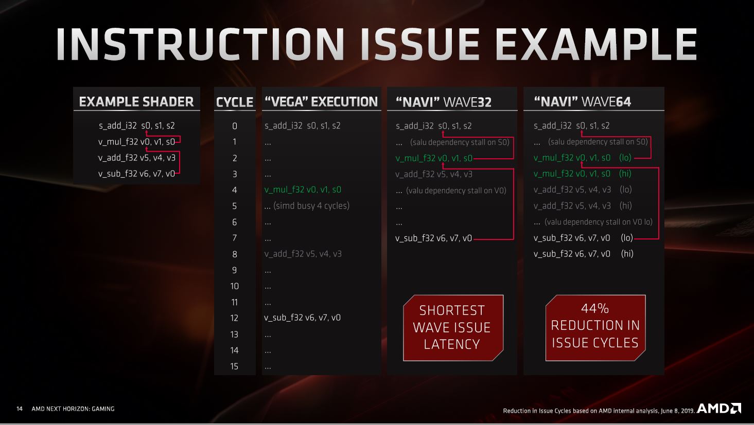
An RDNA compute unit packs 64 stream processors for vector operations and double the number of scalar units for localized serial processing. The stream processors in a CU are split into groups of two, each equipped with a scalar unit. According to AMD, this greatly reduces latency and improves the overall IPC of the compute unit. It also more efficiently utilizes local caches.

The vector execution units, or stream processors, is where much of the GPU's parallel processing happens. Due to the redesigned compute unit, two scalar processors pull two SIMD32 vector units made up of 32 stream processors, each, instead of a single scalar processor pulling four SIMD16 vector units. How is this important? On GCN, the way SIMD units are laid out, all items in a Wave64 operation get to do work once every four clocks due to hardware interleaving. With RDNA, Wave32 work items can do work every clock cycle. In all, RDNA minimizes wasted clock cycles by more efficiently and uniformly utilizing the hardware resources.
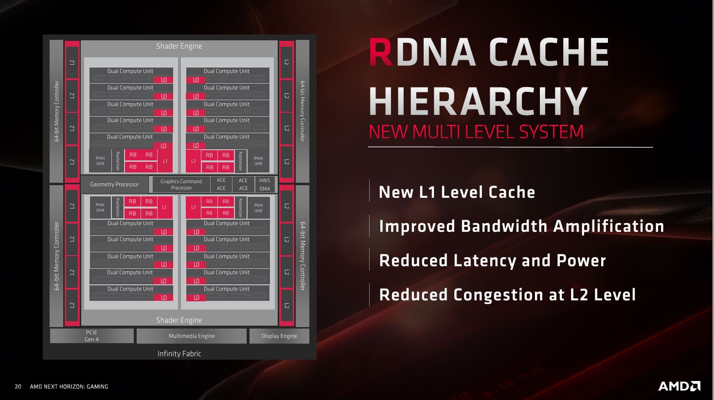
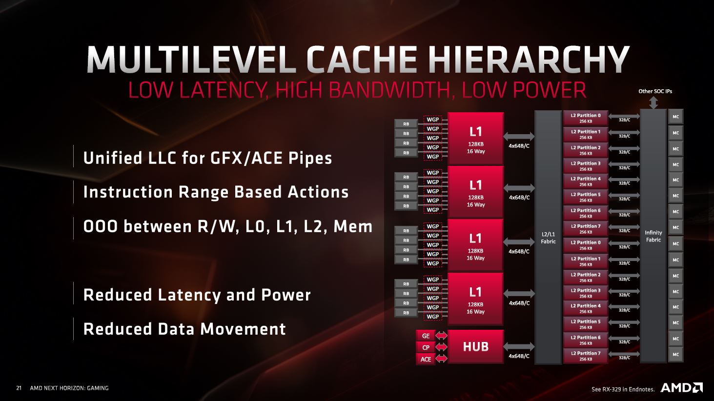
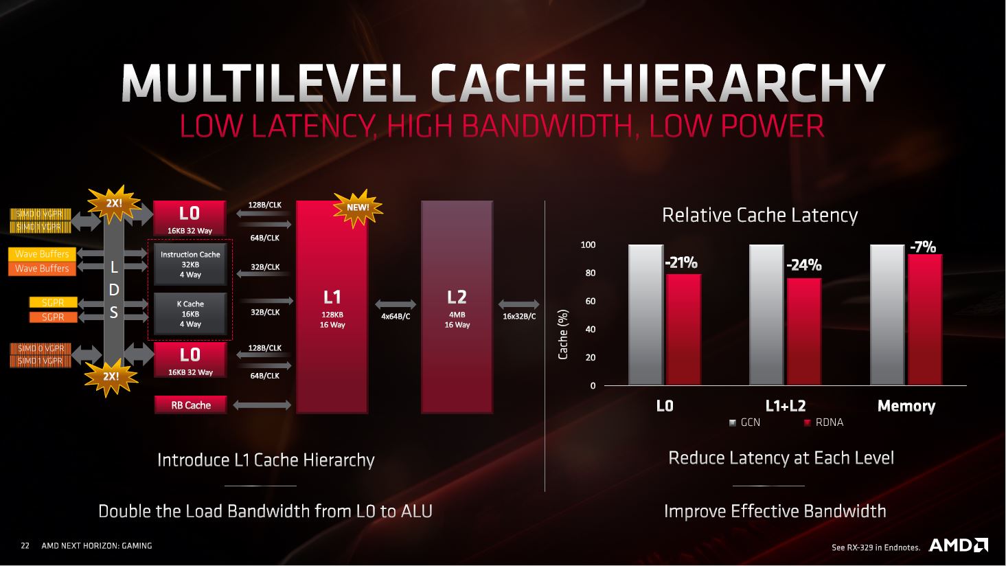

AMD examined previous generations of its graphics architecture to locate bottlenecks in the graphics pipeline. Besides increasing the number of dedicated resources, the company reworked the chip's cache hierarchy by cushioning data transfers at various stages. Each workgroup processor has dedicated 32 KB instruction and 16 KB data caches, which write back to a 128 KB L1 cache dedicated to each Graphics Engine.
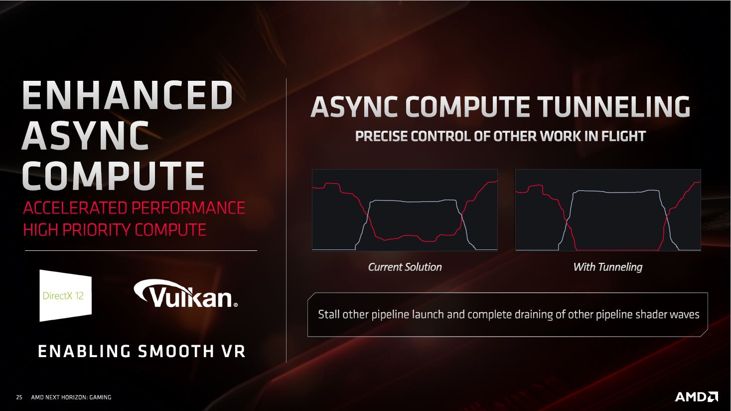
These L1 caches talk to 4 MB of L2 cache. The introduction of the L1 cache and doubling in bandwidth between the various caches contributes greatly to IPC as it minimizes memory accesses, which are much slower than cache accesses. AMD is also using faster (lower latency) SRAM that reduces cache latencies by around 20 percent on die and by 8 percent at the memory level. AMD also introduced new features to the ACEs that include async-compute tunneling.
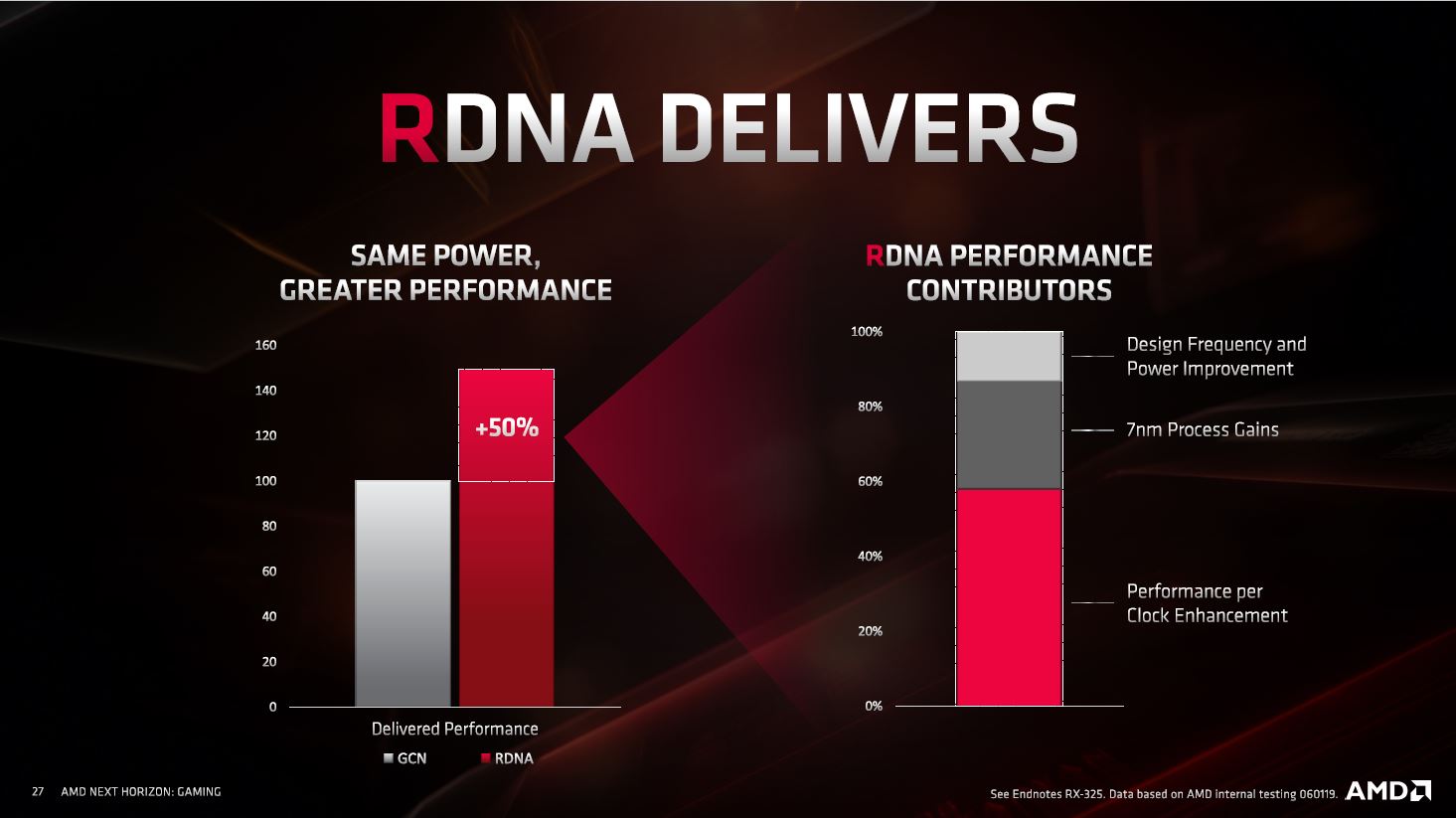
AMD summarizes the benefits of RDNA in a 25 percent IPC gain over the latest version of GCN, and an effective 50 percent performance gain for the GPU when taking into account IPC, the 7 nm process, and gains from the frequency and power management (ability to sustain boost frequencies better).


Elsewhere on the silicon, AMD updated the Display Engine and Multimedia Engine to keep up with the latest display and video standards. The Display Engine now supports DSC 1.2a (display stream compression) along with output standards HDMI 2.0 and DisplayPort 1.4 HDR to support display formats as bandwidth-intensive as 4K 240 Hz or 8K 60 Hz over a single cable, and support for 30 bits per pixel color depth. The multimedia engine supports VP9 and H.265 decoding at up to 8K 24 Hz, or 4K 90 Hz, and hardware-accelerated H.265 encoding at up to 4K 60 Hz.
Features: FidelityFX and Anti-Lag
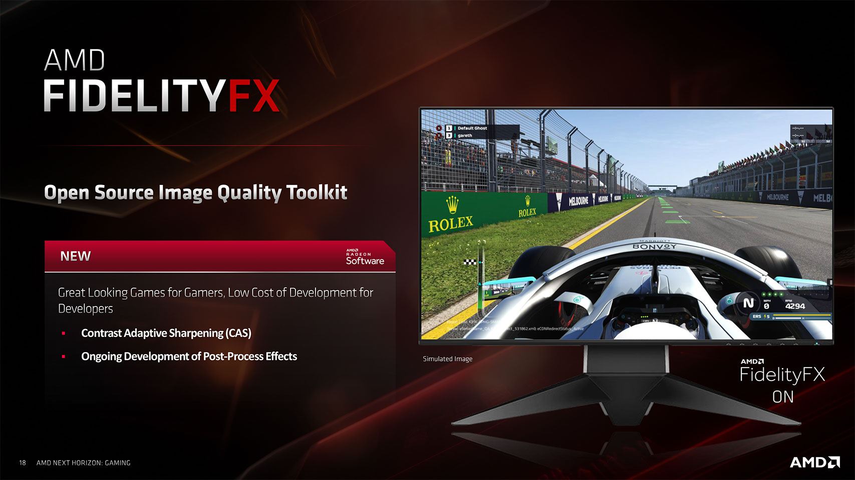

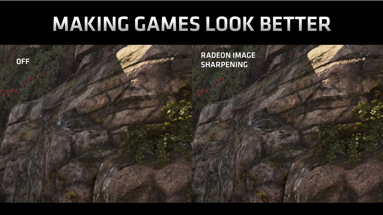

With each new graphics architecture, gamers expect new image quality enhancement features. NVIDIA introduced DLSS, and AMD's response to that is FidelityFX, a combination of content-specific and image-specific quality enhancements. The first part of this is contrast-adaptive sharpening, which brings out details in a scene by enhancing their contrast. To work best, it requires some work from game developers, to declare which parts of the image are to be sharpened (like the HUD and on-screen texts). Details such as wear-lines on the slick tires of a race-car,or hexagonal patterns on a wall come to life. We will test this feature later in a separate article.
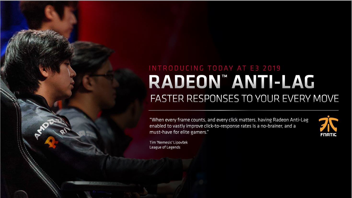


AMD wants to improve its adoption by professional e-Sports gamers by addressing a key bottleneck with modern high-end graphics: mouse-lag. This would be the amount of time taken for a click to register and a response to be rendered by the GPU. Radeon Anti-Lag is a CTR (click-to-response) enhancement that reduced mouse lag by roughly a third across various popular e-Sports titles. This setting is effectively identical to "pre-rendered" frames on NVIDIA. Modern GPUs calculate one or two frames ahead, so they can better time sending them to the monitor to avoid stuttering. Of course, this results in input lag because any input information that comes in only makes it to the screen one or two frames later.
AMD carved the RX 5700 out of the "Navi 10" silicon by randomly disabling two workgroup processors, amounting to four CUs. The resulting stream-processor count is 2,304, and 144 TMUs. The 64 ROPs and memory configuration remain unchanged.
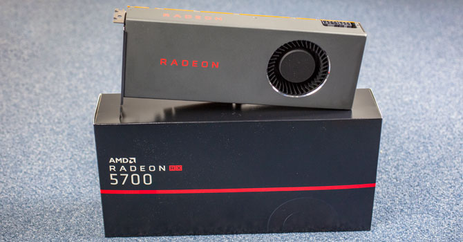
Packaging and Contents


You will receive:
- Graphics card
- Documentation
The Card

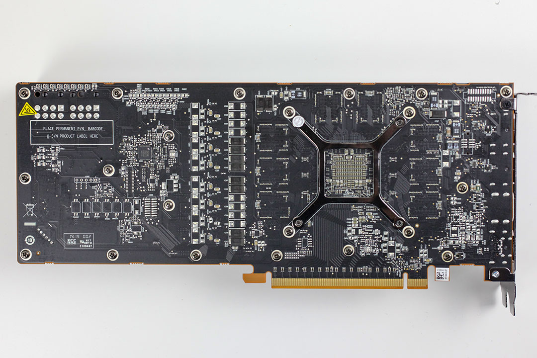
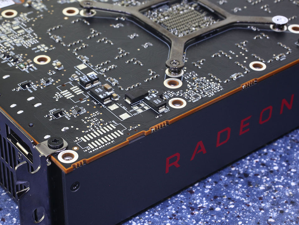
At first glance, the Radeon RX 5700 looks very similar to Vega reference designs if it were not for the gray paint on the cooler. A backplate is not available. Dimensions of the card are 27.0 x 11.0 cm.
Installation requires two slots in your system.

Display connectivity options include three standard DisplayPort 1.4a and an HDMI 2.0b.
AMD took the opportunity to update the display controllers handling these outputs by leveraging DSC 1.2a (display stream compression), which unlocks very high resolution and refresh-rate combinations over a single cable. Among the single-cable display modes supported are 8K 60 Hz (which took two DP 1.3 cables until now), 4K 240 Hz, and 1080p as high as 360 Hz. On top of these, the outputs support HDR and 30 bpc color-depth for better color accuracy in creative applications.
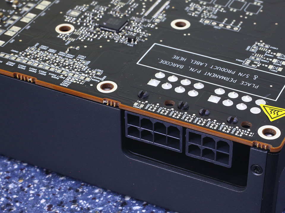
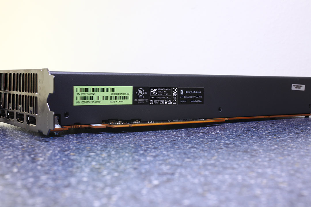
The board uses an 8-pin and a 6-pin power connector. This input configuration is specified for up to 300 watts of power draw.
AMD's Navi generation of GPUs no longer supports CrossFire. DirectX 12 does include its own set of multi-GPU capabilities, but using it requires game developers to put serious development time into a feature only a tiny fraction of their customers might ever use.
Our Patreon Silver Supporters can read articles in single-page format.
Apr 19th, 2024 05:38 EDT
change timezone
Latest GPU Drivers
New Forum Posts
- Should the CDPR make the Fallout 5 instead? (26)
- Linus watercools (23)
- Roccat Kone AIMO has developed a double left click, when I click it once. Any fix out there? (28)
- First computer build for my son (3)
- FFMPEG commands for advanced enhanced image & video editing & conversion? (0)
- Do you use Linux? (230)
- Unlocked Realtek HD Audio Drivers for Windows 11 (Dolby Digital Live/DTS Interactive) (154)
- Ghetto Mods (4318)
- Identify my GPU - RX 570 8GB (or what?) (3)
- FINAL FANTASY XIV: Dawntrail Official Benchmark (58)
Popular Reviews
- Horizon Forbidden West Performance Benchmark Review - 30 GPUs Tested
- PowerColor Radeon RX 7900 GRE Hellhound Review
- Fractal Design Terra Review
- Corsair 2000D Airflow Review
- Minisforum EliteMini UM780 XTX (AMD Ryzen 7 7840HS) Review
- Thermalright Phantom Spirit 120 EVO Review
- Creative Pebble X Plus Review
- FiiO KB3 HiFi Mechanical Keyboard Review - Integrated DAC/Amp!
- ASUS GeForce RTX 4090 STRIX OC Review
- NVIDIA GeForce RTX 4090 Founders Edition Review - Impressive Performance
Controversial News Posts
- Sony PlayStation 5 Pro Specifications Confirmed, Console Arrives Before Holidays (110)
- NVIDIA Points Intel Raptor Lake CPU Users to Get Help from Intel Amid System Instability Issues (102)
- US Government Wants Nuclear Plants to Offload AI Data Center Expansion (98)
- Windows 10 Security Updates to Cost $61 After 2025, $427 by 2028 (82)
- Developers of Outpost Infinity Siege Recommend Underclocking i9-13900K and i9-14900K for Stability on Machines with RTX 4090 (82)
- TechPowerUp Hiring: Reviewers Wanted for Motherboards, Laptops, Gaming Handhelds and Prebuilt Desktops (71)
- Intel Realizes the Only Way to Save x86 is to Democratize it, Reopens x86 IP Licensing (70)
- AMD Zen 5 Execution Engine Leaked, Features True 512-bit FPU (63)