 715
715
AMD Ryzen 7 5800X3D Review - The Magic of 3D V-Cache
Unboxing & Photos »AMD 3D Vertical Cache Technology
The star attraction with AMD Ryzen 7 5800X3D is the 3D Vertical Cache technology (3DV cache). Without it, the processor isn't architecturally different from the Ryzen 7 5800X. This is still very much the Zen 3 and not the "Zen 3+" microarchitecture used in Ryzen 6000 "Rembrandt" processors. As we mentioned in the introduction, 3D Vertical Cache is an attempt at lubricating the memory sub-system of Zen 3, so the increased capacity of the last-level cache could improve performance of not just multi-threaded streaming data workloads, but also IPC-sensitive workloads, such as games.
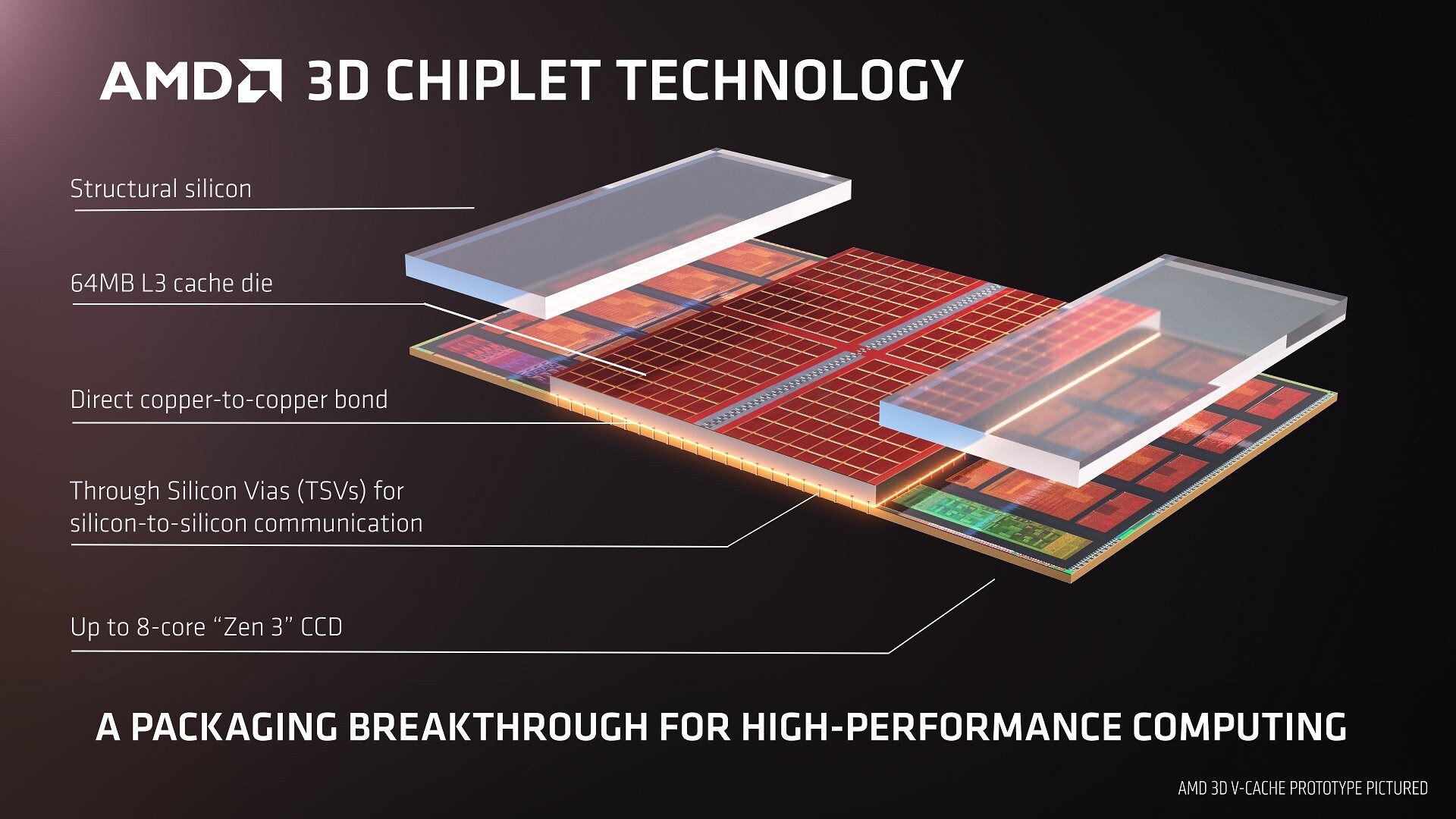
The Ryzen 7 5800X3D comes with 96 MB of L3 cache thanks to the 3DV cache. Notice we said it's 96 MB, and not 32+64 MB. This is because the 32 MB on-die cache and 64 MB 3DV cache are stacked on top of the die, form a contiguously addressable block of L3 cache. Both the CPU cores and software (OS) are shown 96 MB of L3 cache, at least that's the idea. AMD says that for the best performance, you need to use the latest AMD Chipset Software (version 4.03.03.431 or later). This probably means some degree of "awareness" is still needed at the OS-level, or the chipset driver has some other minor optimization. The Ryzen 5800X3D is drop-in compatible with existing Socket AM4 motherboards with a UEFI firmware that packs AGESA V2 1.2.0.6b microcode (or later).
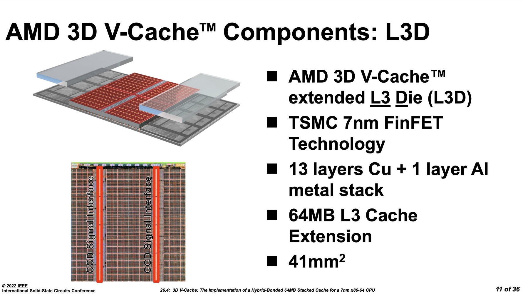
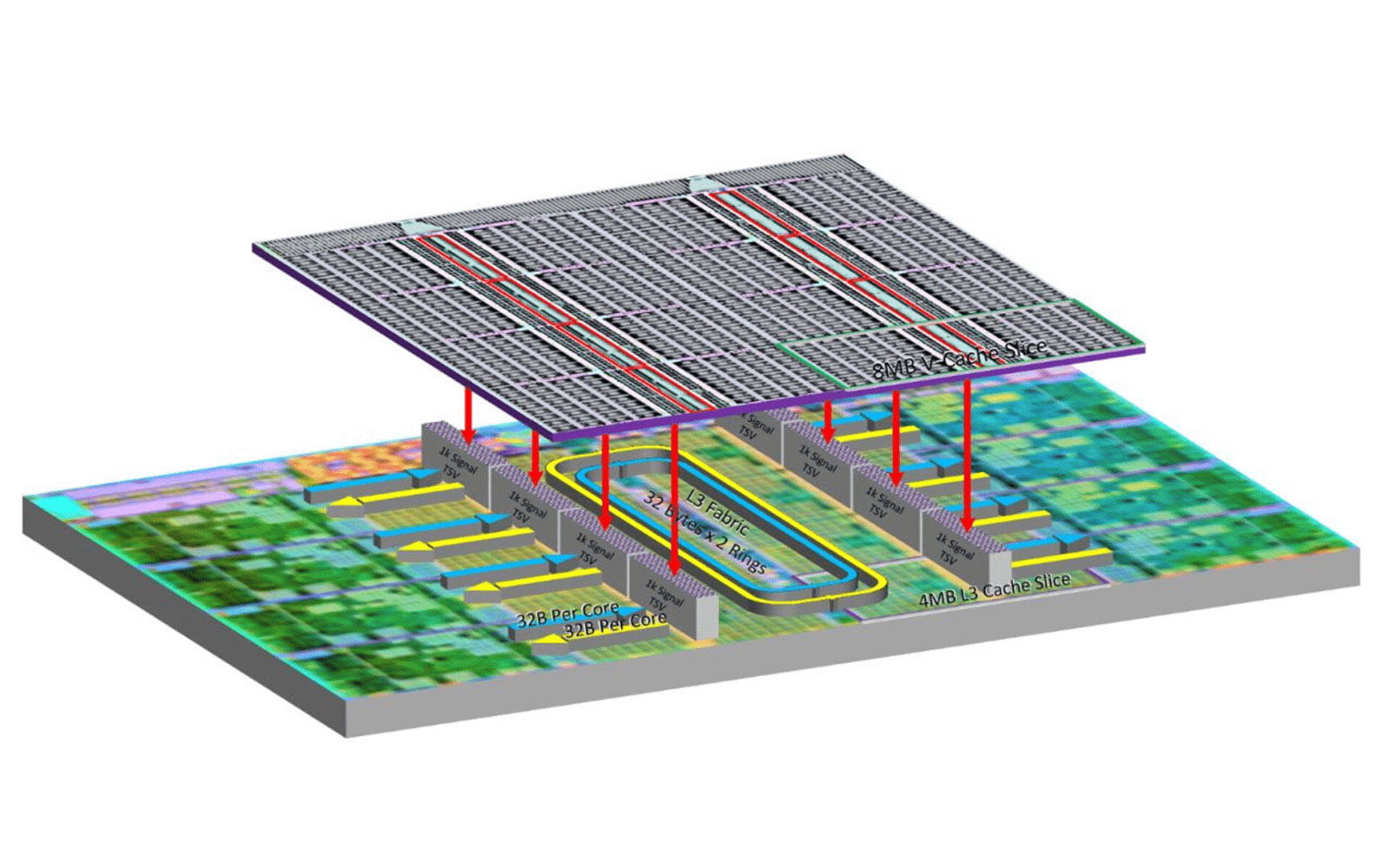
Built on the same 7 nm node as the rest of the CCD, the 3DV cache die (L3D) is a chunk of fast SRAM—the same physical media as the on-die 32 MB L3 cache. The various SRAM banks on this die are interconnected using a bi-directional ringbus of the CCD. This is what makes the CPU cores and software see 96 MB of addressable L3 cache as opposed to the 64 MB 3DV cache serving as an "L4 cache" (an additional tier of cache) to the L3. Much like the on-die 32 MB L3 cache, the 3DV cache operates at the CPU frequency. The L3D measures 41 mm² in area, which is roughly half that of the CCD underneath.

AMD co-engineered the Zen 3 with 3DV cache chiplet with TSMC, its principal foundry partner. The company used two TSMC innovations to create it. First, the CCD die was "thinned," or built on a thinner silicon substrate. Intel resorted to similar die-thinning for its 10th Gen "Comet Lake" silicon to make room for a thicker IHS. In AMD's case, the vertical space gained from die-thinning accommodates the 64 MB 3DV cache die. This die is stacked above the region of the CCD that has the 32 MB on-die cache. The vertical gap created between the CCD region with the CPU cores is filled up with structural silicon, which conducts heat to the sTIM and IHS. The 3DV cache die and CCD below are physically connected through direct copper-to-copper bonding, and TSVs, through silicon vias. A via is an electrical connection that passes through a substrate, such as a silicon die or fiberglass PCB.
The Zen 3 Microarchitecture
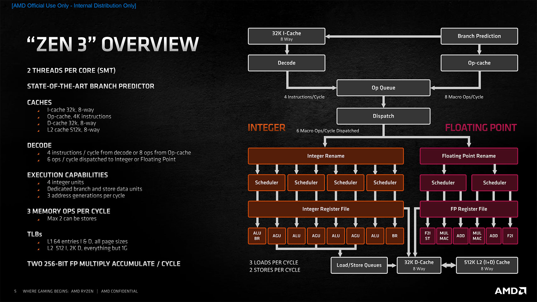
Since its 2017 debut, AMD has delivered a new iteration of its groundbreaking Zen CPU microarchitecture each year, each with IPC improvements. As we mentioned earlier, the new Zen 3 microarchitecture claims to offer a massive 19 percent IPC uplift over its predecessor, Zen 2. This is accomplished by improvements at both the micro and macro levels. We already detailed the macro (beyond the core) changes above. In this section, we talk about what's new inside each core. AMD mentioned updates to practically all key components of the core, including its front-end, fetch/decode, integer and floating-point components, load-store, and dedicated caches. Just to clarify, this component is unchanged compared to other Zen 3 CPUs without an IGP, like the Ryzen 9 5900X.
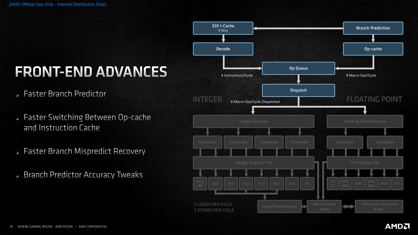
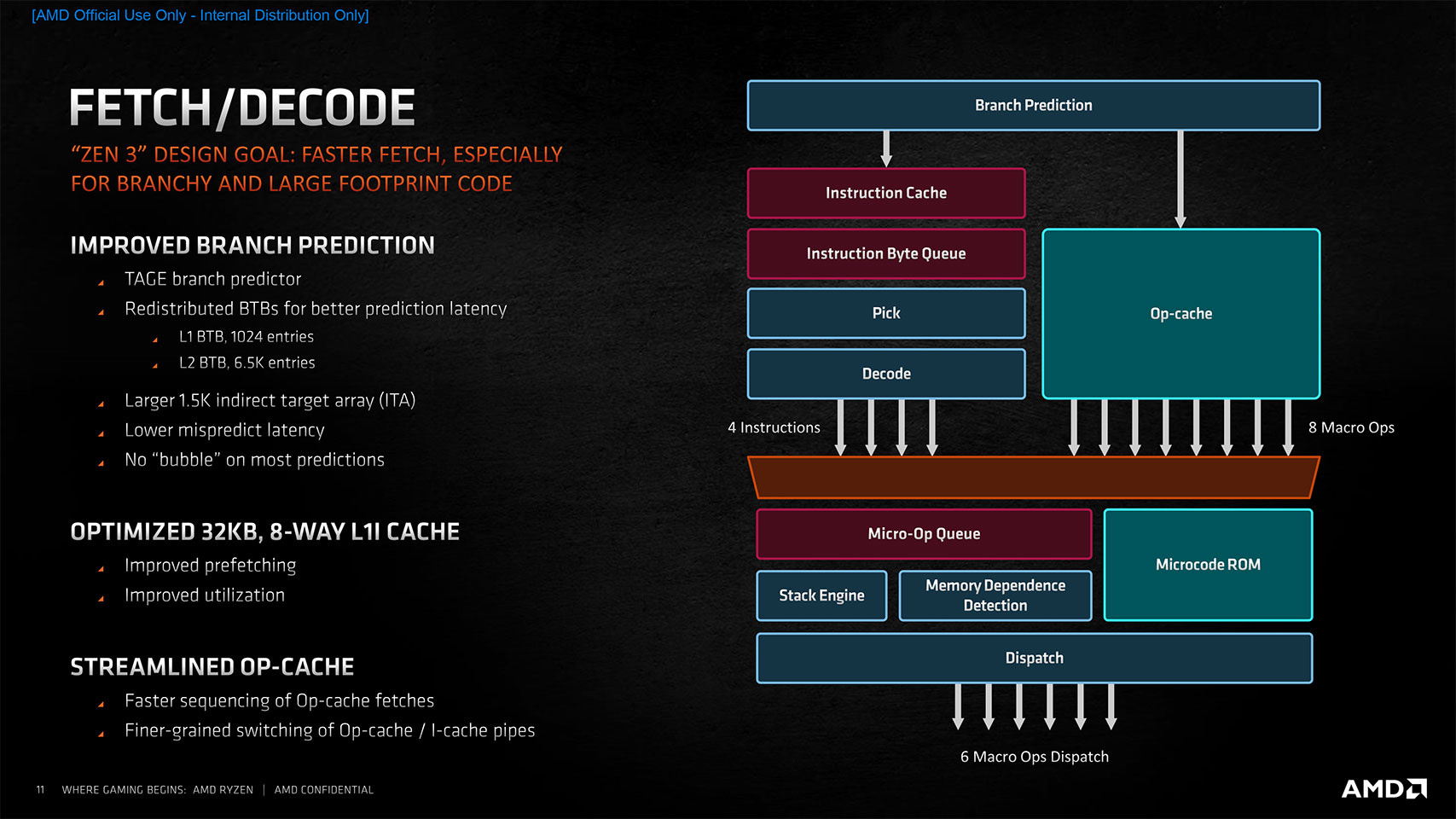
Modern processors execute multiple instructions in parallel to improve performance. Computer programs consist of huge amounts of "if ... then ... else" instructions, which slow down the processor because it has to evaluate the condition before picking a branch to execute. In order to overcome this limitation, the branch predictor was invented, a piece of circuitry that takes a guess on the more likely outcome of the condition check and speculatively executes that branch's instructions. Of course, there's a chance that the prediction is wrong, in which case a performance penalty is incurred from undoing the already executed executions. With Zen 3, AMD uses an improved TAGE branch predictor, which is more accurate and recovers faster from mispredictions. They also changed the design to be "bubble free," which avoids inserting "wait for result" instructions into the instruction stream whenever a branch is encountered.
AMD generally increased operations per cycle; the front-end now switches between the op and instruction caches faster. The 32 KB L1 instruction cache has been tweaked to offer better utilization due to efficient tagging and pre-fetching. Streamlining was done to the Op cache. Improvements to the branch predictor and front-end add up to nearly a quarter of the overall 19% generational IPC uplift.
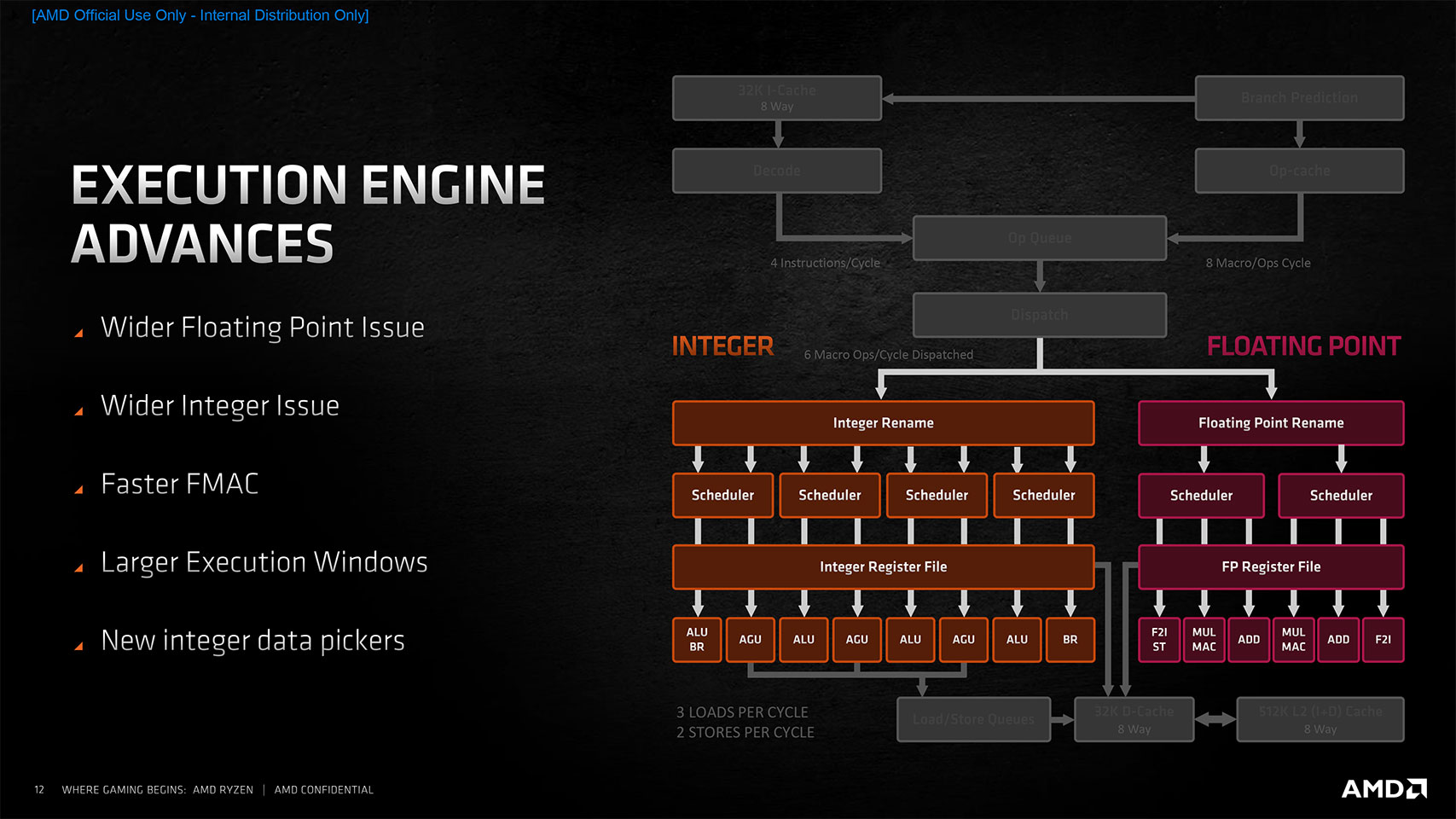
The execution engine, or combination of the integer and floating-point execution units, is the main math muscle of the CPU core. The Zen 3 microarchitecture features improvements to both over Zen 2. Both the INT and FP issue queues, which feed work to the two engines, have been widened and the execution window enlarged. This ensures fewer units are idle in typical programs, which increases overall performance.


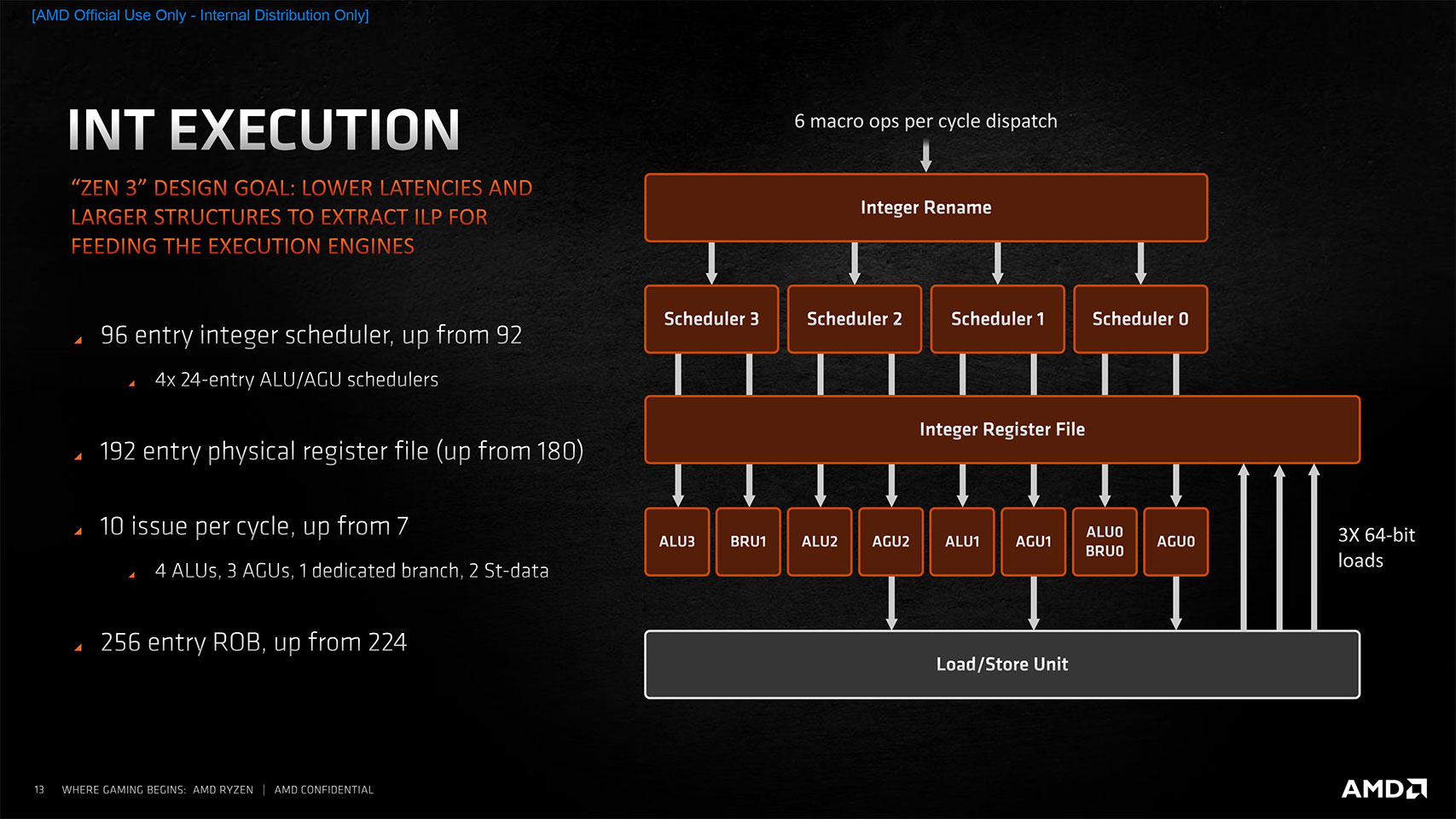
AMD worked to minimize latencies at every stage of the INT execution engine and enlarged its key structures, including the integer scheduler (96 entry vs. 92 on Zen 2), physical register file (192 vs. 180 on Zen 2), and 10 issues per cycle, up from 7 on Zen 2. Data picker bandwidth has been significantly increased despite the same number of ALUs. The floating-point engine features the same 256-bit FPUs, but just as with the INT engine, the FP engine has latency and bandwidth improvements across the board, a faster 4-cycle FMAC, and a larger scheduler. The INT and FP improvements contribute around a fifth of the 19% overall IPC uplift.
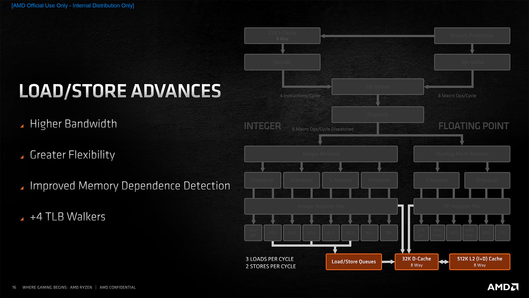

With the Zen 3 microarchitecture, AMD addressed many bottlenecks and "intelligence" issues with the Load/Store unit. The biggest has to be bandwidth. The entry store queue has been widened to 64 from 48 on Zen 2, and the L2 cache DTLB is 2K entries wide. The 32 KB L1 data cache has been made faster with lower latencies. Memory dependence detection has been improved. Much like the front end and scheduler, the load/store improvements contribute nearly a quarter of the 19% overall IPC uplift, meaning that by just optimizing the non-execution components of its core, AMD managed to pull off a vast 9% overall IPC uplift.
ISA and Security Changes


Each new microarchitecture heralds support for newer instruction sets and security hardening, and the same is the case with Zen 3; however, a notable absentee is AVX-512. Granted, Intel has adopted a less than perfect method of proliferating AVX-512 with certain instructions being exclusive to enterprise-segment microarchitectures and only a handful client-relevant instructions on its "Ice Lake" and "Tiger Lake" architectures, but there's no movement from AMD in this direction.
You still do get 256-bit instructions from within the AVX2 set. Also missing in action is something to rival Intel's DLBoost, which is essentially a software exposure of fixed-function hardware that accelerates matrix multiplication; in effect, AI deep-learning neural net building and training. A lot of client applications, particularly image manipulation and video editing, are leveraging edge AI, and some investment from AMD on this would have been nice. That said, Zen 3 adds two new ISA instructions, MPK (memory protection keys) and AVX2 support for AES/APCLMulQD. AMD has been ahead of Intel with CPU core security vulnerability perception, and with Zen 3, AMD is introducing CET, or control-flow enforcement, which should provide hardening against ROP-type attacks.
AMD X570 and B550 Chipsets
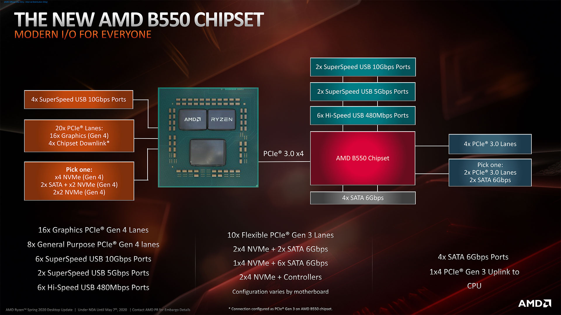

AMD Ryzen 5000 Zen 3 processors are compatible with all Socket AM4 motherboards based on AMD X570 and B550 chipsets, besides the AMD 400-series. AMD also recently announced that official (not beta) Ryzen 5000 support will be introduced to 300-series around May to June. The B550 and X570 chipsets are still recommended for this processor as motherboards based on them give you PCI-Express Gen 4 connectivity, which is particularly useful for the latest crop of SSDs.
The AMD X570 chipset is a premium offering that enables PCI-Express gen 4.0 not just from the processor (i.e., the main x16 PEG slot and one M.2 NVMe slot), but also downstream PCIe lanes attached to the chipset. You get up to 16 PCIe gen 4 lanes from the chipset, which can be re-configured as SATA or USB3 ports by the motherboard designer. The B550 chipset lets you have one PCIe gen 4 main x16 slot and one M.2 NVMe slot, but all chipset-attached downstream lanes are PCIe gen 3. The B550 puts out eight downstream lanes. When paired with 5000G Cezanne processors, the downstream PCIe lanes of the X570 operate at Gen 3 speeds despite being capable of Gen 4.
Apr 25th, 2024 08:25 EDT
change timezone
Latest GPU Drivers
New Forum Posts
- i7-12800HX Overheating Issues (0)
- Intel ARC Firmware Compilation Matrix (22)
- Alphacool CORE 1 CPU block - bulging with danger of splitting? (6)
- Bizarre Throttlestop issue (6)
- (Anti) SFF fun house (353)
- Core i5-6300U (17)
- Last game you purchased? (255)
- Share your AIDA 64 cache and memory benchmark here (2916)
- What phone you use as your daily driver? And, a discussion of them. (1472)
- What's your latest tech purchase? (20338)
Popular Reviews
- Fractal Design Terra Review
- Thermalright Phantom Spirit 120 EVO Review
- Corsair 2000D Airflow Review
- Minisforum EliteMini UM780 XTX (AMD Ryzen 7 7840HS) Review
- ASUS GeForce RTX 4090 STRIX OC Review
- NVIDIA GeForce RTX 4090 Founders Edition Review - Impressive Performance
- ASUS GeForce RTX 4090 Matrix Platinum Review - The RTX 4090 Ti
- MSI GeForce RTX 4090 Suprim X Review
- MSI GeForce RTX 4090 Gaming X Trio Review
- Gigabyte GeForce RTX 4090 Gaming OC Review
Controversial News Posts
- Sony PlayStation 5 Pro Specifications Confirmed, Console Arrives Before Holidays (116)
- NVIDIA Points Intel Raptor Lake CPU Users to Get Help from Intel Amid System Instability Issues (106)
- AMD "Strix Halo" Zen 5 Mobile Processor Pictured: Chiplet-based, Uses 256-bit LPDDR5X (101)
- US Government Wants Nuclear Plants to Offload AI Data Center Expansion (98)
- Windows 11 Now Officially Adware as Microsoft Embeds Ads in the Start Menu (87)
- Developers of Outpost Infinity Siege Recommend Underclocking i9-13900K and i9-14900K for Stability on Machines with RTX 4090 (85)
- Windows 10 Security Updates to Cost $61 After 2025, $427 by 2028 (84)
- AMD's RDNA 4 GPUs Could Stick with 18 Gbps GDDR6 Memory (81)