 8
8
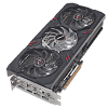
ASRock Radeon RX 7600 Phantom Gaming Review
Test Setup »High-resolution PCB Pictures
These pictures are for the convenience of volt modders and people who would like to see all the finer details on the PCB. Feel free to link back to us and use these in your articles, videos or forum posts.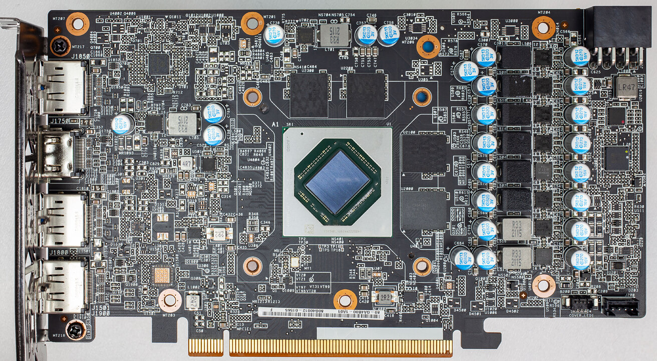
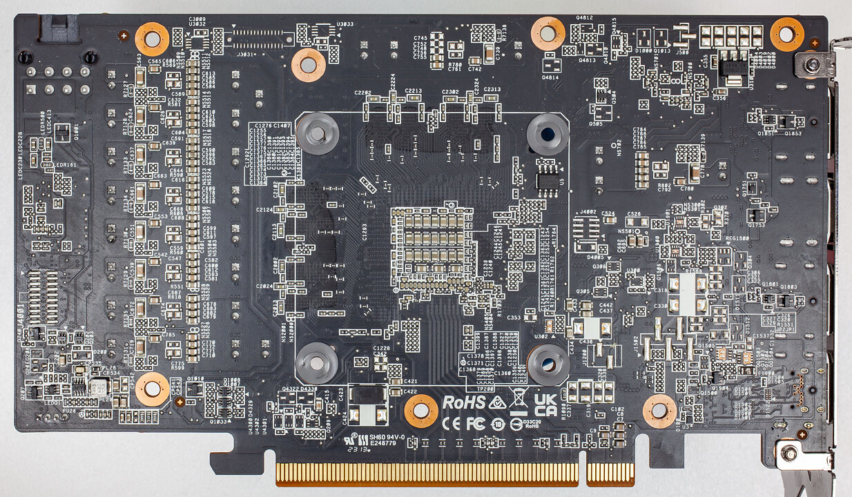
High-resolution versions are also available (front, back).
Circuit Board (PCB) Analysis


GPU voltage is an 8-phase design, managed by a IRF 35217 controller.
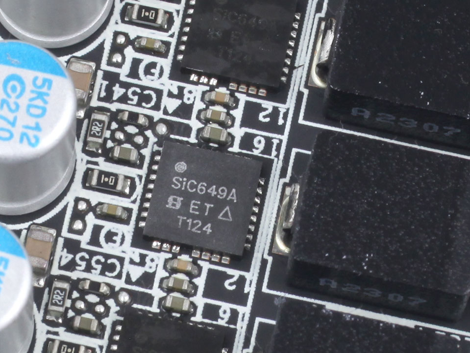
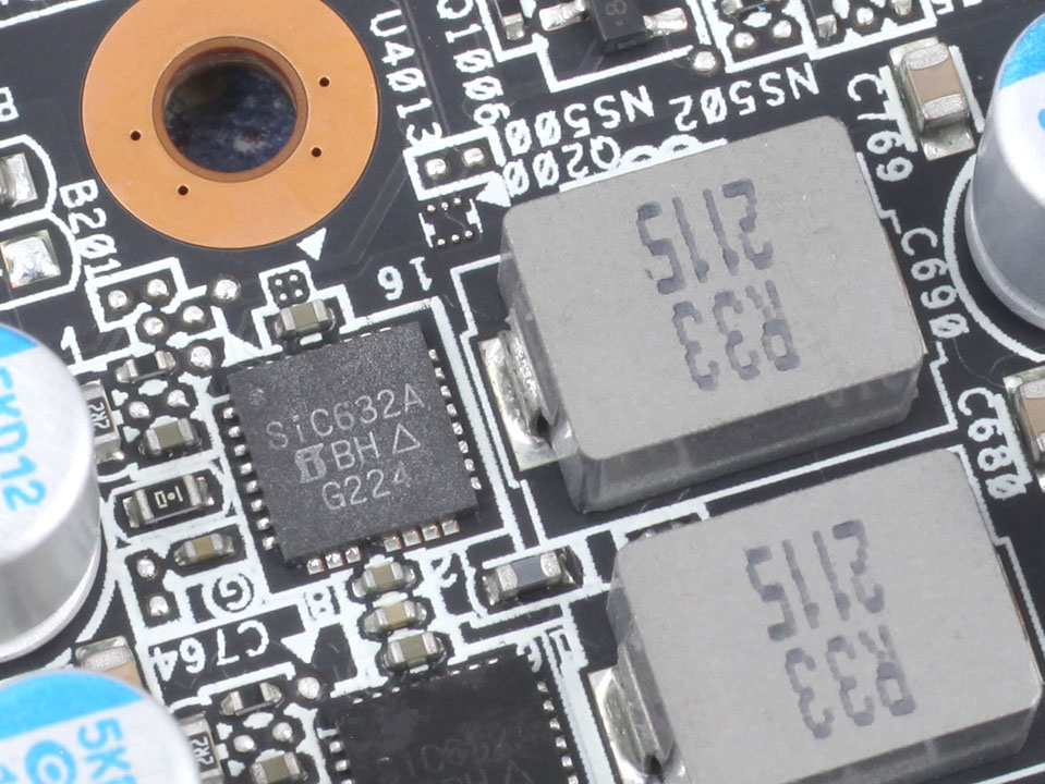
GPU voltage on AMD is two separate rails. On one, Vishay SiC649A chips are used, the other rail uses Vishay SiC632A are used.


Memory voltage uses a two-phase design and is generated by an NCP81022N controller.
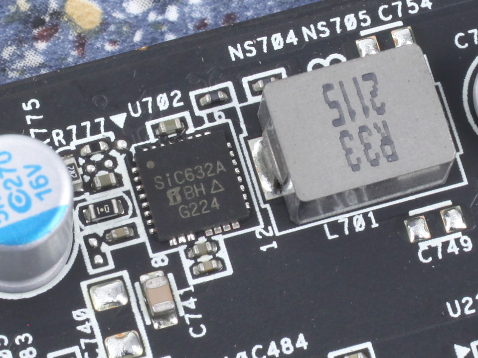
For memory, 45 A-capable Vishay SiC632A DrMOS chips are used.

The GDDR6 memory chips are made by Hynix and carry the model number H56G42AS8DX-014. They are specified to run at 2500 MHz (20 Gbps effective).
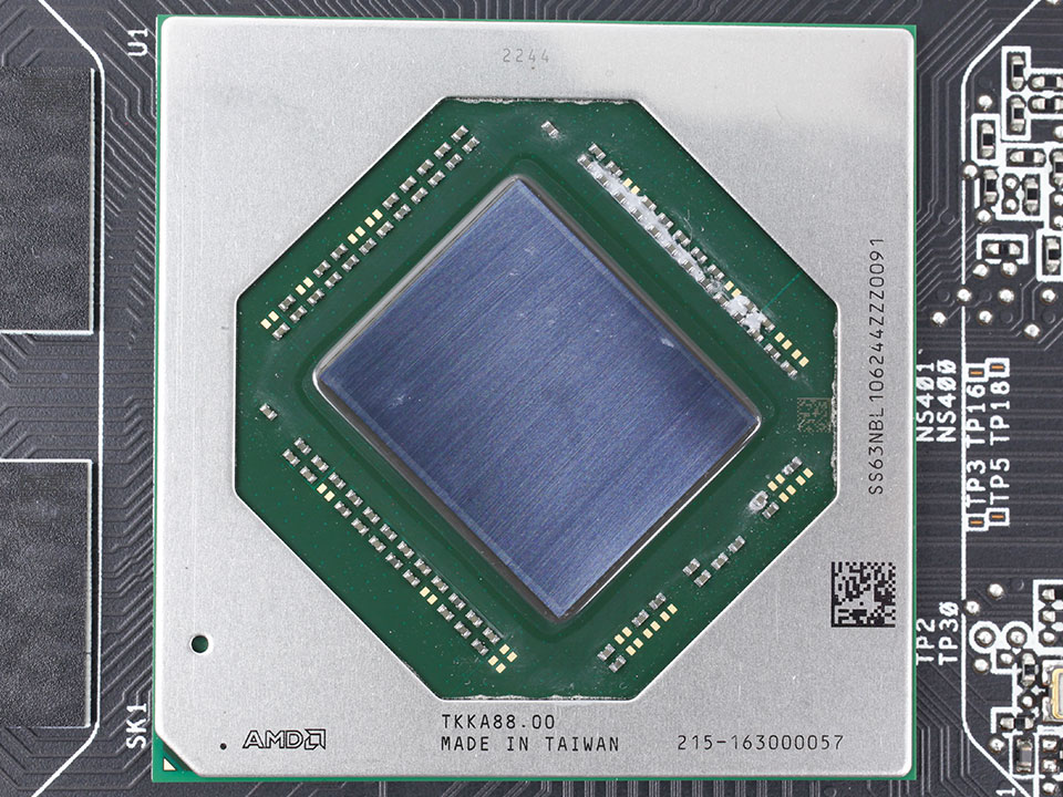
AMD's new Navi 33 graphics processor is a monolithic design, unlike Navi 31, which powers the RX 7900 Series. It is fabricated on a 6 nm process at TSMC Taiwan with a die size of 204 mm² and 13.3 billion transistors.
May 11th, 2024 04:46 EDT
change timezone
Latest GPU Drivers
New Forum Posts
- Flash VBIOS to turn RX 580 2048SP into RX 570 (36)
- Should I install Windows 10 or 11 for my new device (69)
- What's your latest tech purchase? (20502)
- Motherboard only has one USB header, i need possibly four! can I use a splitter cable? (0)
- NVME underperforming (8)
- Who here likes big monitors? 42inch and bigger gang? (7)
- RM750x (2021) enough for my 5800X3D + 7900XT system? (18)
- The Filthy, Rotten, Nasty, Helpdesk-Nightmare picture clubhouse (2625)
- 2024 and STILL no dark mode? (15)
- AM5 boot times improve RADICALLY with memory context restore enabled (40)
Popular Reviews
- Bykski CPU-XPR-C-I CPU Water Block Review - Amazing Value!
- CHERRY XTRFY M64 Pro Review
- ThundeRobot ML903 NearLink Review
- ZMF Caldera Closed Planar Magnetic Headphones Review
- Corsair MP700 Pro SE 4 TB Review
- Corsair iCUE Link RX120 RGB 120 mm Fan Review
- Upcoming Hardware Launches 2023 (Updated Feb 2024)
- AMD Ryzen 7 7800X3D Review - The Best Gaming CPU
- Finalmouse UltralightX Review
- ASUS Radeon RX 7900 GRE TUF OC Review
Controversial News Posts
- Intel Statement on Stability Issues: "Motherboard Makers to Blame" (265)
- AMD to Redesign Ray Tracing Hardware on RDNA 4 (206)
- Windows 11 Now Officially Adware as Microsoft Embeds Ads in the Start Menu (171)
- NVIDIA to Only Launch the Flagship GeForce RTX 5090 in 2024, Rest of the Series in 2025 (144)
- Sony PlayStation 5 Pro Specifications Confirmed, Console Arrives Before Holidays (119)
- AMD's RDNA 4 GPUs Could Stick with 18 Gbps GDDR6 Memory (114)
- NVIDIA Points Intel Raptor Lake CPU Users to Get Help from Intel Amid System Instability Issues (106)
- AMD Ryzen 9 7900X3D Now at a Mouth-watering $329 (104)