 33
33
ASRock Radeon RX 7900 XTX Taichi White Review - O_o Sexy
(33 Comments) »Introduction
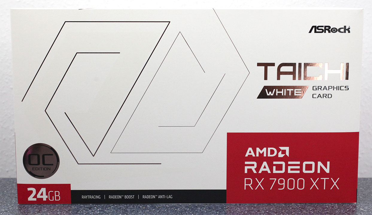
ASRock Radeon RX 7900 XTX Taichi White is a special edition of the company's top air-cooled graphics card that's suitable for boutique gaming PC builds with an all-white theme. This is ASRock's first such graphics card, although the white-theme can be had with the company's Taichi Carrara series motherboards, such as the Z790 Taichi Carrara and the X670E Taichi Carrara. We have also reviewed the regular ASRock RX 7900 XTX Taichi OC a while ago, this review is the white version. The AMD Radeon RX 7900 XTX is the fastest graphics card from Team-Red, and rocks the latest AMD RDNA 3 graphics architecture. The company is promising to repeat a generational 50% performance/Watt increase like it had with the RX 6000 series, which would put the company back in competition with NVIDIA's fastest GeForce RTX 40-series "Ada" GPUs, such as the RTX 4080, and occasionally even the RTX 4090.
The RDNA 3 graphics architecture debuts the world's first chiplets-based gaming GPU. The "Navi 31" ASIC at the heart of the RX 7900 XTX sees the core number-crunching and graphics rendering machinery of the GPU placed on a large central die based on the 5 nm process, called the Graphics Compute Die (GCD), while the parts of the GPU that don't benefit as much from the switch to the latest foundry process, namely the Infinity Cache memory, and the memory controllers, are disintegrated into six chiplets surrounding the GCD. Each chiplet has a 16 MB segment of the GPU's 96 MB of Infinity Cache, and a 64-bit GDDR6 memory interface; and is hence called the Memory Cache Die (MCD). There are six of these, making up the GPU's 384-bit GDDR6 memory interface, handling 24 GB of memory.

The RDNA 3 graphics architecture debuts a new-generation Compute Unit with dual instruction issue-rate SIMD components, support for new math formats, AI acceleration integrated at the CU-level, and 2nd generation Ray Accelerators that improve ray tracing performance over the previous generation. AMD claims a 17.5% IPC uplift over RDNA2 compute units, which when combined with generationally increased clock-speeds, and a 20% increase in CU counts over "Navi 21," form the bedrock of the performance uplift over the previous generation, with the company claiming to have retained the streak of 50% performance/Watt uplift with each generation of RDNA. With a 50% wider memory interface and proportionately larger memory, the GPU's reliance on the Infinity Cache isn't as much, and so it is reduced in size to 96 MB (compared to 128 MB on the RX 6900 XT). AMD is also using faster 20 Gbps-rated GDDR6 memory, which means the total memory bandwidth is now all the way up to 960 GB/s, a massive 87% generational increase.
As we mentioned earlier, the ASRock Taichi White is a color-scheme based variant of the company's original RX 7900 XTX Taichi OC. Both cards offer the same factory overclocked speed of 2510 MHz game clocks, and 2680 MHz boost (compared to 2269 MHz game and 2499 MHz boost); while the memory is left untouched at 20 Gbps (GDDR6-effective). Matte white replaces gunmetal-gray on all the gunmetal-colored bits of the original RX 7900 XTX Taichi, including the cooler shroud, the fan impellers, and the backplate. The underlying PCB is still black, but that's barely noticeable. The card draws power from three 8-pin PCIe power connectors, for a total power input capability of 525 W, which means the GPU enjoys much better boost frequency residency, particularly to sustain the factory-overclock. ASRock is pricing the RX 7900 XTX Taichi White at $1,120, a small $40 premium over the original Taichi price of $1080, and $120 higher than the $999 AMD MSRP.
| Price | Cores | ROPs | Core Clock | Boost Clock | Memory Clock | GPU | Transistors | Memory | |
|---|---|---|---|---|---|---|---|---|---|
| RTX 2080 Ti | $420 | 4352 | 88 | 1350 MHz | 1545 MHz | 1750 MHz | TU102 | 18600M | 11 GB, GDDR6, 352-bit |
| RTX 3070 | $400 | 5888 | 96 | 1500 MHz | 1725 MHz | 1750 MHz | GA104 | 17400M | 8 GB, GDDR6, 256-bit |
| RTX 3070 Ti | $520 | 6144 | 96 | 1575 MHz | 1770 MHz | 1188 MHz | GA104 | 17400M | 8 GB, GDDR6X, 256-bit |
| RX 6800 | $480 | 3840 | 96 | 1815 MHz | 2105 MHz | 2000 MHz | Navi 21 | 26800M | 16 GB, GDDR6, 256-bit |
| RX 6800 XT | $560 | 4608 | 128 | 2015 MHz | 2250 MHz | 2000 MHz | Navi 21 | 26800M | 16 GB, GDDR6, 256-bit |
| RTX 3080 | $570 | 8704 | 96 | 1440 MHz | 1710 MHz | 1188 MHz | GA102 | 28000M | 10 GB, GDDR6X, 320-bit |
| RTX 3080 Ti | $750 | 10240 | 112 | 1365 MHz | 1665 MHz | 1188 MHz | GA102 | 28000M | 12 GB, GDDR6X, 384-bit |
| RX 6900 XT | $680 | 5120 | 128 | 2015 MHz | 2250 MHz | 2000 MHz | Navi 21 | 26800M | 16 GB, GDDR6, 256-bit |
| RX 6950 XT | $800 | 5120 | 128 | 2100 MHz | 2310 MHz | 2250 MHz | Navi 21 | 26800M | 16 GB, GDDR6, 256-bit |
| RTX 3090 | $850 | 10496 | 112 | 1395 MHz | 1695 MHz | 1219 MHz | GA102 | 28000M | 24 GB, GDDR6X, 384-bit |
| RTX 4070 Ti | $820 | 7680 | 80 | 2310 MHz | 2610 MHz | 1313 MHz | AD104 | 35800M | 12 GB, GDDR6X, 192-bit |
| RX 7900 XT | $880 | 5376 | 192 | 2000 MHz | 2400 MHz | 2500 MHz | Navi 31 | 57700M | 20 GB, GDDR6, 320-bit |
| RTX 3090 Ti | $1400 | 10752 | 112 | 1560 MHz | 1950 MHz | 1313 MHz | GA102 | 28000M | 24 GB, GDDR6X, 384-bit |
| RTX 4080 | $1200 | 9728 | 112 | 2205 MHz | 2505 MHz | 1400 MHz | AD103 | 45900M | 16 GB, GDDR6X, 256-bit |
| RX 7900 XTX | $1000 | 6144 | 192 | 2300 MHz | 2500 MHz | 2500 MHz | Navi 31 | 57700M | 24 GB, GDDR6, 384-bit |
| ASRock RX 7900 XTX Taichi | $1120 | 6144 | 192 | 2510 MHz | 2680 MHz | 2500 MHz | Navi 31 | 57700M | 24 GB, GDDR6, 384-bit |
| RTX 4090 | $1600 | 16384 | 176 | 2235 MHz | 2520 MHz | 1313 MHz | AD102 | 76300M | 24 GB, GDDR6X, 384-bit |
Packaging
The Card

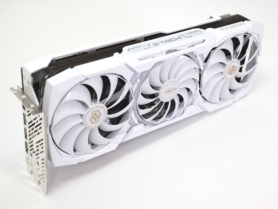
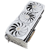
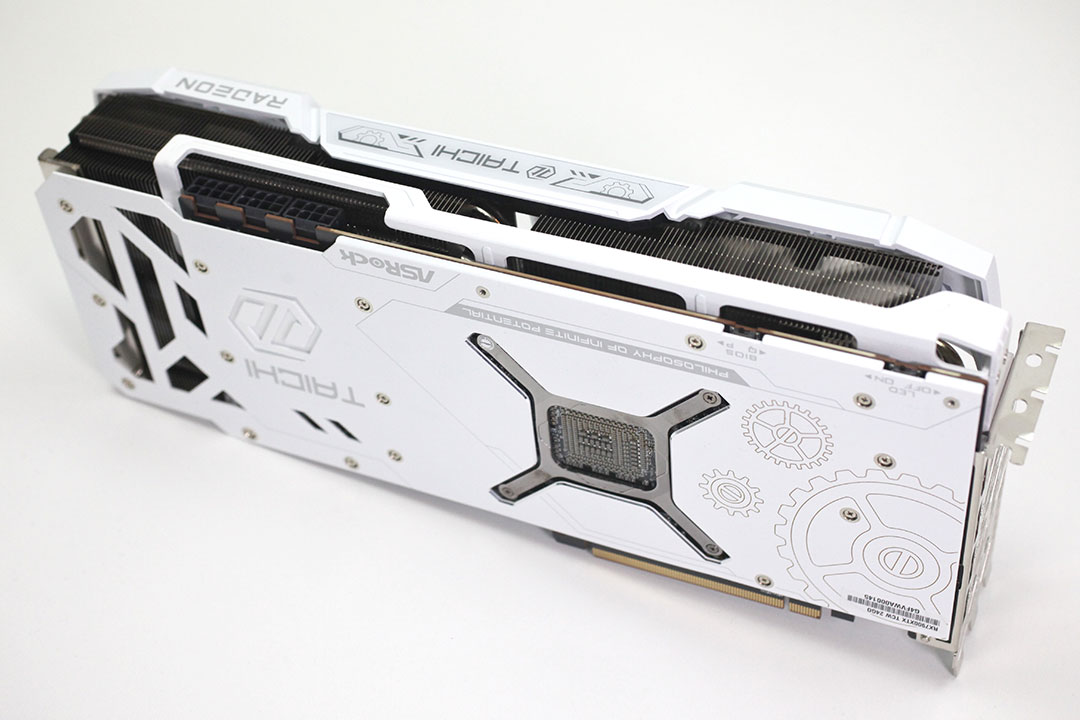
ASRock created a new design for their RX 7900 Series Taichi cooler. They kept the blocky, industrial design of previous Taichi products, but the cogwheel iconography is now only present on the center fan hub. The fan frames are now solid, which helps make the card look less busy. On the metal backplate we get to meet the cogwheel design again, ASRock has added more white highlights here compared to previous generations.
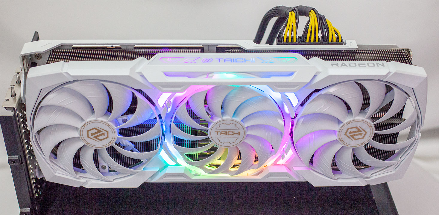

ASRock has placed two RGB zones in the front cooler, one along the top edge, the second near the middle fan. On the back you get a third RGB element that illuminates the Taichi logo.
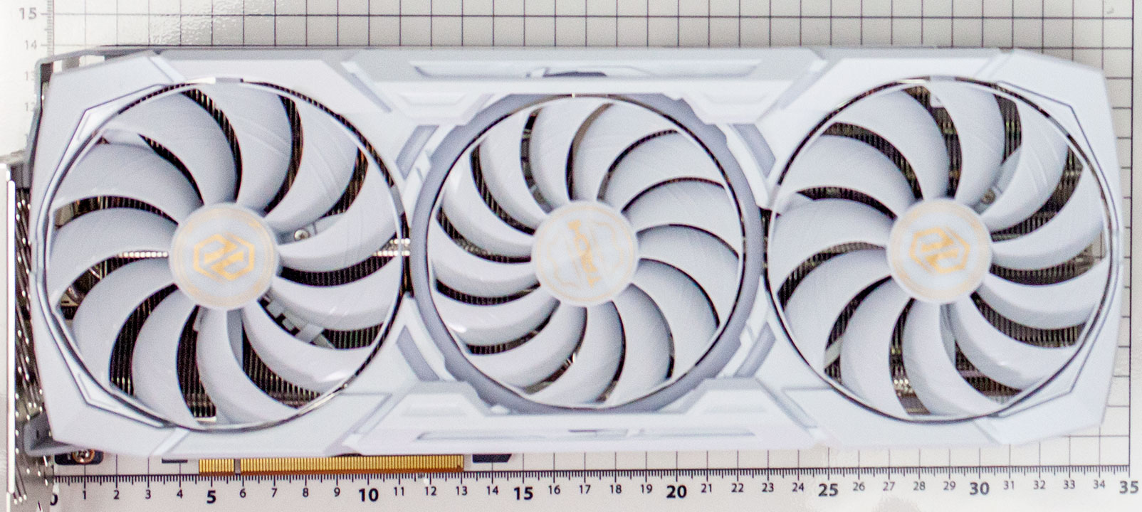
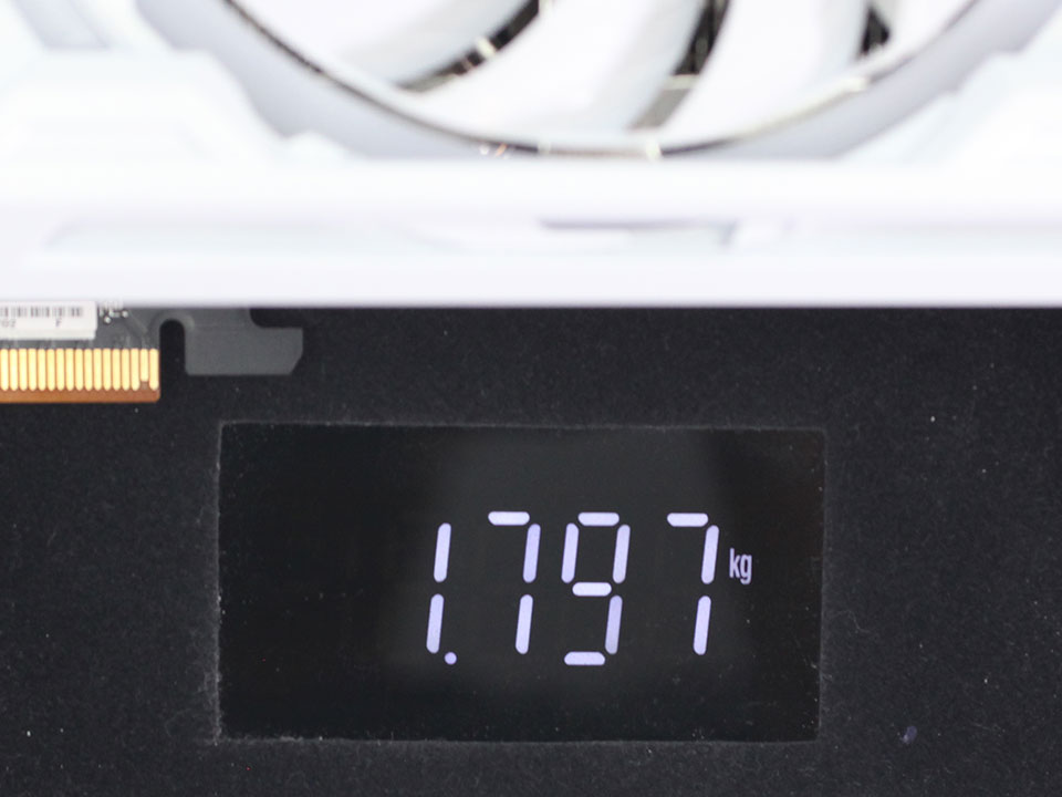
Dimensions of the card are 35.0 x 14.0 cm, and it weighs 1772 g.
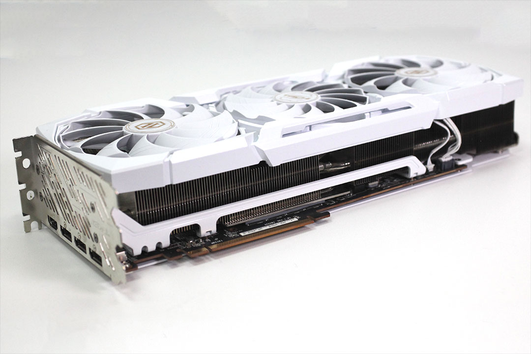
Installation requires three slots in your system.
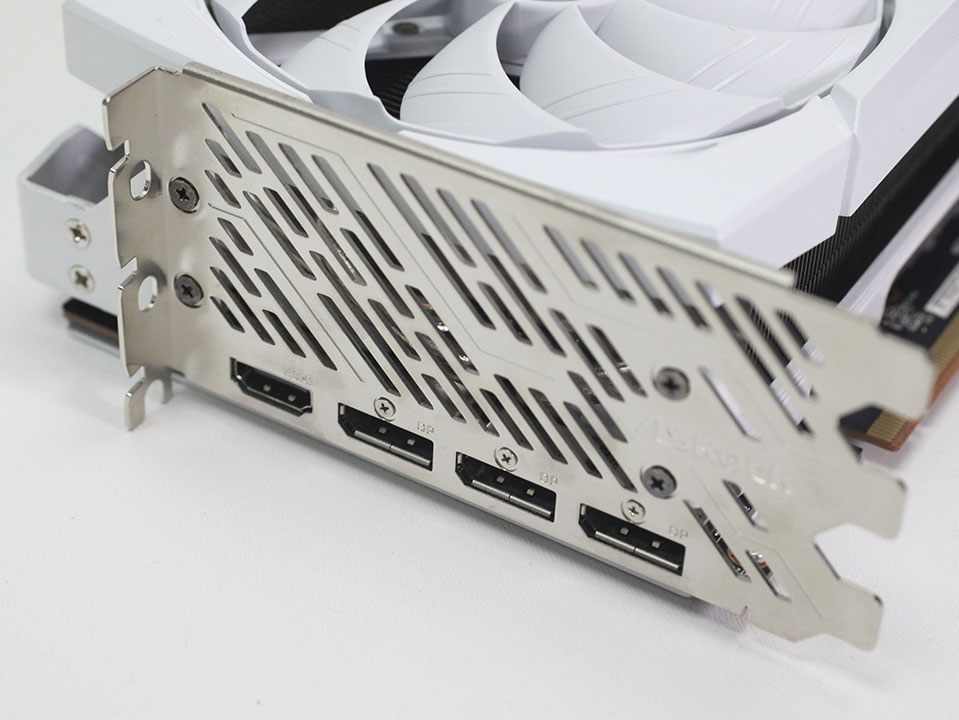
Display connectivity includes two standard DisplayPort 2.1 ports (RDNA2 had 1.4a) and two HDMI 2.1a (same as RDNA2).
AMD has upgraded their encode/decode setup. It now comes with two independent hardware units that can encode and decode two streams of video in parallel, or one stream at double the FPS rate. There's support for VP9, H.264, H.265 and AV1 decode, and encoding is supported for H.264, H.265 and AV1.
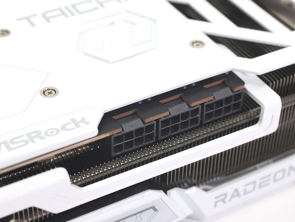
The card uses a classic triple 8-pin power input config, rated for 525 W maximum power. NVIDIA on the other hand uses the new 12+4 pin ATX 12VHPWR connector, which is rated for up to 600 W of power draw.

Near the power connectors you'll find a 3-pin ARGB header, which lets you sync the graphics card lighting effects to the rest of your system.
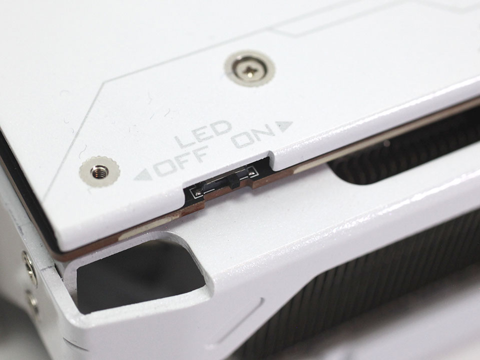
I love this! A dedicated switch lets you turn off the RGB lighting—no software needed.
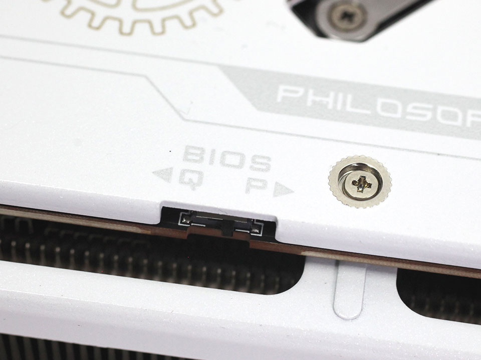
The dual BIOS feature lets you switch between the default "Performance" BIOS and a "Quiet" BIOS. While other vendors reduce the fan speed and allow higher temperatures, ASRock has decided to reduce clocks and voltages instead, which lowers heat output, which makes it easier for the fans to cool the card. This means that both Performance and Quiet mode are running at the same temperatures. Quiet mode is roughly 4% slower, but considerably quieter.
Teardown


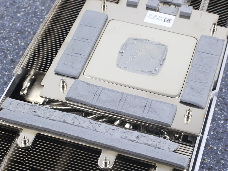
ASRock has engineered an excellent thermal solution that uses eight heatpipes to move heat away quickly from the GPU. The main cooler also provides cooling for the VRM and memory chips.
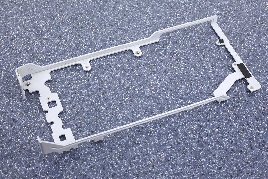
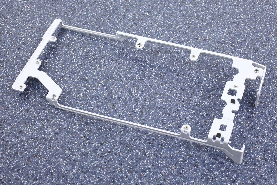
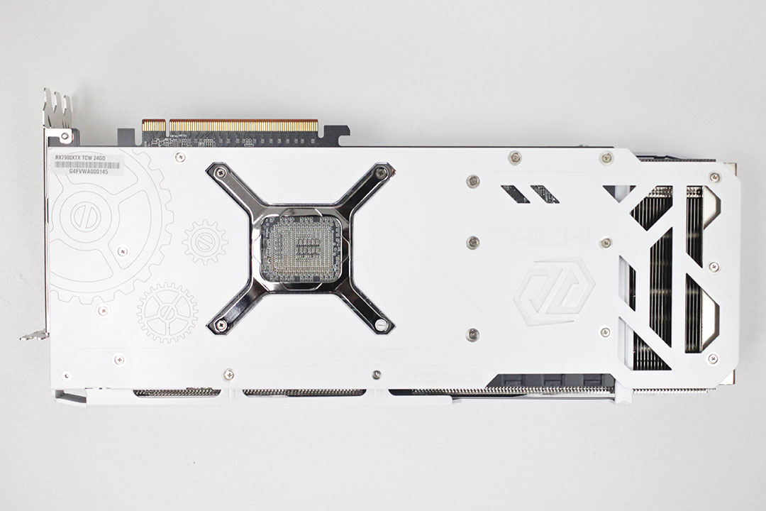
Once the main cooler is removed, a metal reinforcement brace appears, which helps strengthen the card, to protect against warping and sagging.
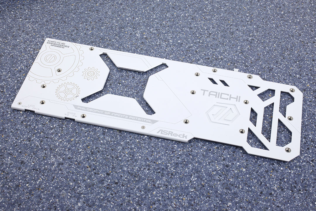

The backplate is made of metal and protects the card against damage during installation and handling.
High-resolution PCB Pictures
These pictures are for the convenience of volt modders and people who would like to see all the finer details on the PCB. Feel free to link back to us and use these in your articles, videos or forum posts.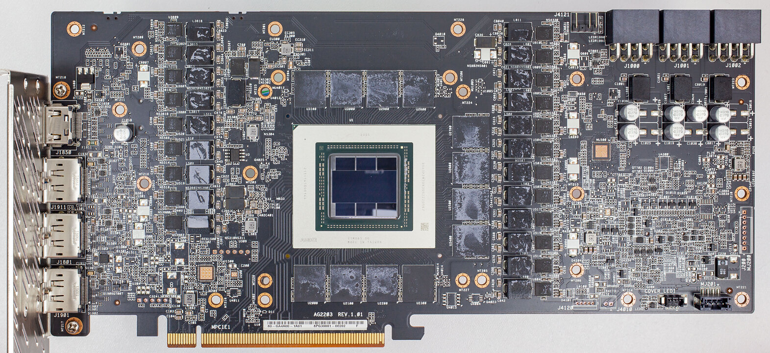
High-resolution versions are also available (front, back).
Circuit Board (PCB) Analysis
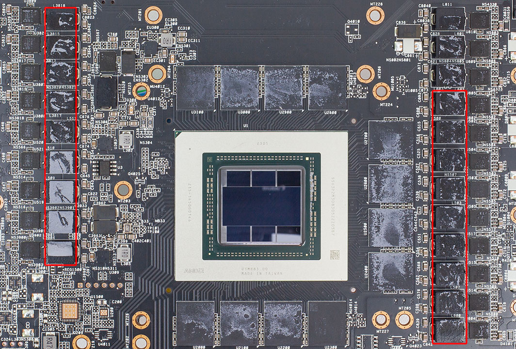
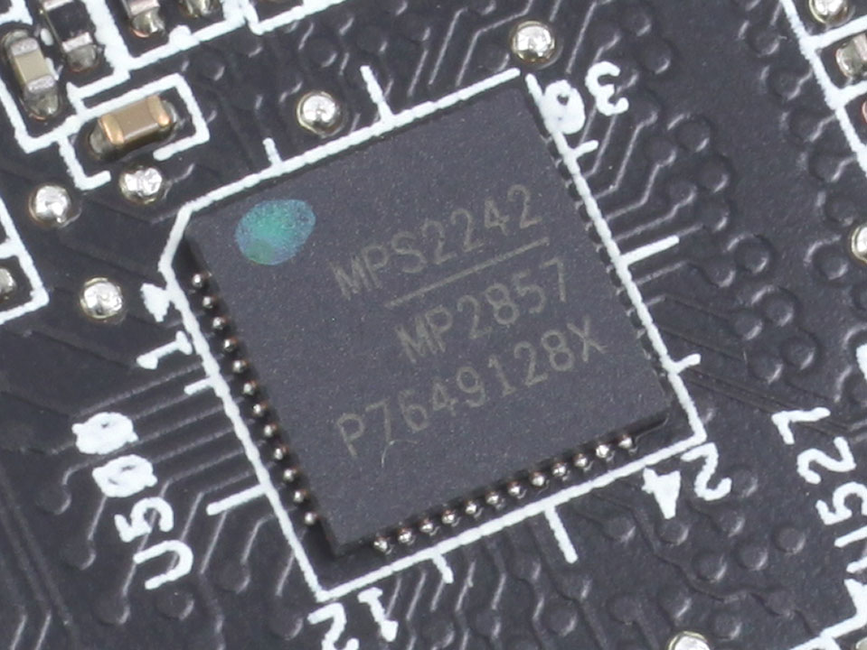
GPU voltage is a 18-phase design, managed by a Monolithic Power Systems MP2857 controller.
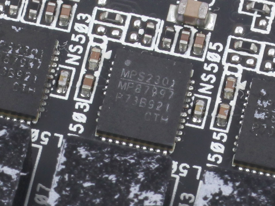
Monolithic MP87997 DrMOS components are used for GPU voltage; they are rated for 70 A of current each.


Memory voltage is a four-phase design, managed by a Monolithic Power Systems MP2856 controller.
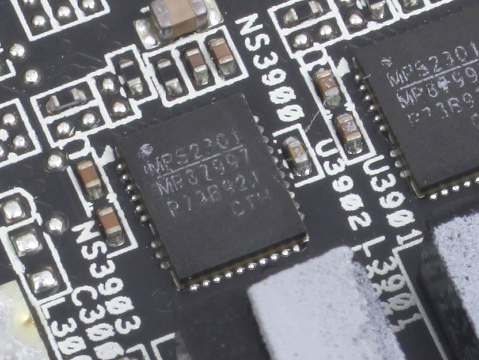
For memory, Monolithic MP87997 DrMOS with a 70 A rating are used again.
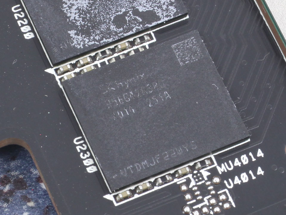
The GDDR6 memory chips are made by Hynix and carry the model number H56G42AS8DX-014. They are specified to run at 2500 MHz (20 Gbps effective).
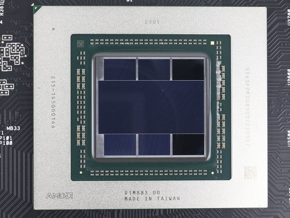
AMD's new Navi 31 graphics processor is the world's first GPU that uses a chiplet architecture. Note the large die in the center, called "GCD," graphics compute die, which houses the compute units, it is surrounded by six smaller "MCD," memory cache dies, that contain one memory controller interface and one slice of cache each. While they look similar, the MCDs are not HBM chips. The MCDs are fabricated on a 6 nm process at TSMC Taiwan with a die size of 36.6 mm² each, the GCD is fabricated using TSMC's 5 nanometer node, with a die size of 300 mm². The combined transistor count of the GPU is 57.7 billion.
Our Patreon Silver Supporters can read articles in single-page format.
May 15th, 2024 22:59 EDT
change timezone
Latest GPU Drivers
New Forum Posts
- Ryzen Owners Zen Garden (7363)
- Last game you purchased? (296)
- RTX 4090 VS Titan Volta or titan RTX (7)
- MSI Z370 SLI PLUS + i9 9900k bad perfomance. (0)
- RMAd every single component in my PC, and it's still crashing (14)
- 20 Years? (14)
- I just succesfully baked DDR4 (96)
- Homeworld 3 [Official Thread] (41)
- Air makes its way from the reservoir into the radiator. (79)
- Double radiator setup with GPU fans on top (0)
Popular Reviews
- Homeworld 3 Performance Benchmark Review - 35 GPUs Tested
- Enermax REVOLUTION D.F. X 1200 W Review
- Upcoming Hardware Launches 2023 (Updated Feb 2024)
- Lofree Edge Ultra-Low Profile Wireless Mechanical Keyboard Review
- ZMF Caldera Closed Planar Magnetic Headphones Review
- AMD Ryzen 7 7800X3D Review - The Best Gaming CPU
- Corsair MP700 Pro SE 4 TB Review
- ASUS Radeon RX 7900 GRE TUF OC Review
- ThundeRobot ML903 NearLink Review
- Sapphire Radeon RX 7900 GRE Pulse Review
Controversial News Posts
- Intel Statement on Stability Issues: "Motherboard Makers to Blame" (267)
- AMD to Redesign Ray Tracing Hardware on RDNA 4 (227)
- Windows 11 Now Officially Adware as Microsoft Embeds Ads in the Start Menu (172)
- NVIDIA to Only Launch the Flagship GeForce RTX 5090 in 2024, Rest of the Series in 2025 (152)
- AMD Hits Highest-Ever x86 CPU Market Share in Q1 2024 Across Desktop and Server (137)
- AMD RDNA 5 a "Clean Sheet" Graphics Architecture, RDNA 4 Merely Corrects a Bug Over RDNA 3 (124)
- AMD's RDNA 4 GPUs Could Stick with 18 Gbps GDDR6 Memory (114)
- AMD Ryzen 9 7900X3D Now at a Mouth-watering $329 (104)