 126
Intel Panther Lake Technical Deep Dive
Compute Tile: CPU Architecture »Panther Lake Configurations


The Panther Lake system-on-chip is built from three tiles: a compute tile, a graphics tile, and a platform controller tile. The compute tile is fabricated on Intel's 18A process. The graphics tile exists in two versions—one produced on Intel 3 and another, larger variant manufactured by TSMC. The platform controller tile, which integrates connectivity and I/O functions, is also produced by TSMC. All three tiles are linked by Intel's second-generation scalable fabric, allowing them to operate as a single coherent system while being made on different process nodes. The exact processes used are: compute (Intel 18A); 12-Xe GPU (TSMC N3E); 4-Xe GPU (Intel 3); PCT/PCH (TSMC N6). This is an interesting mix and shows a definite move back towards Intel's own manufacturing. In the past we've seen them rely heavily on TSMC.
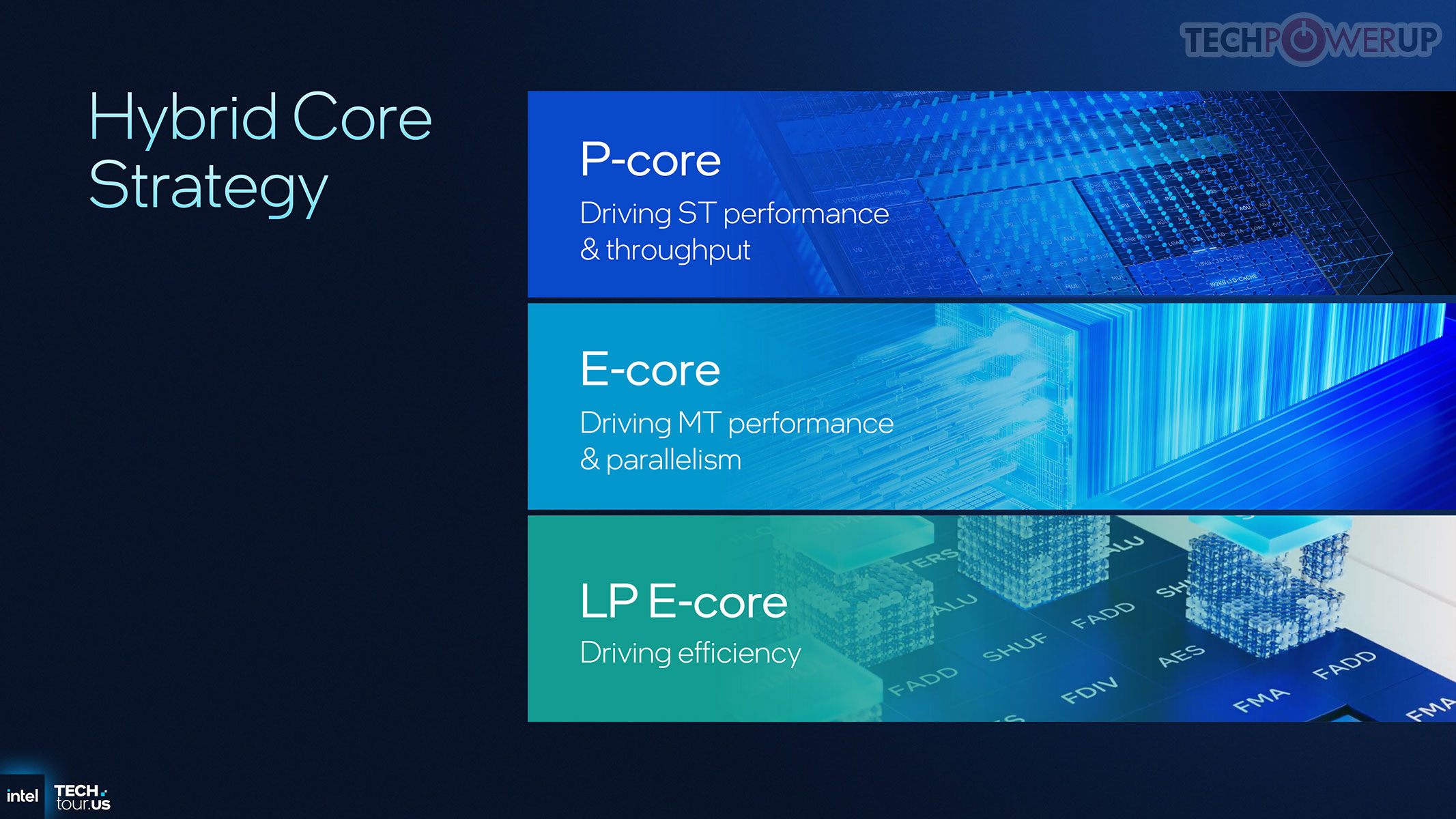

The compute tile combines several types of cores: four Cougar Cove performance cores (marked blue with "P"), eight Darkmont efficiency cores on the 4+8+4 die (marked light-blue with "E"), and four low-power efficiency cores (marked greenish with "LPE"). All cores are located on the compute tile and connected through a unified ring bus that provides shared access to cache and memory resources. This arrangement improves communication between core clusters and lowers latency compared with previous client designs, where core types were connected through separate interconnects.

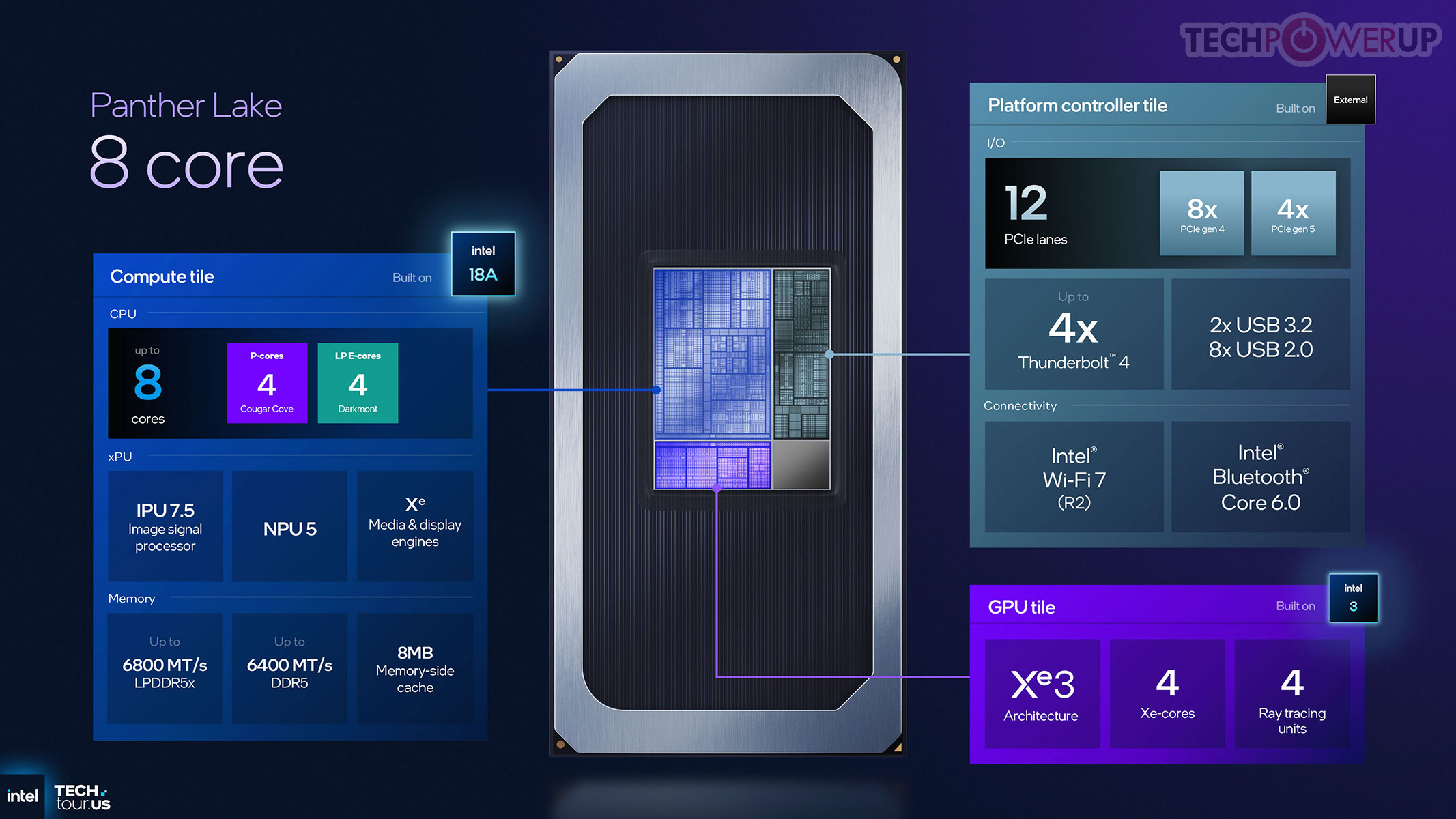
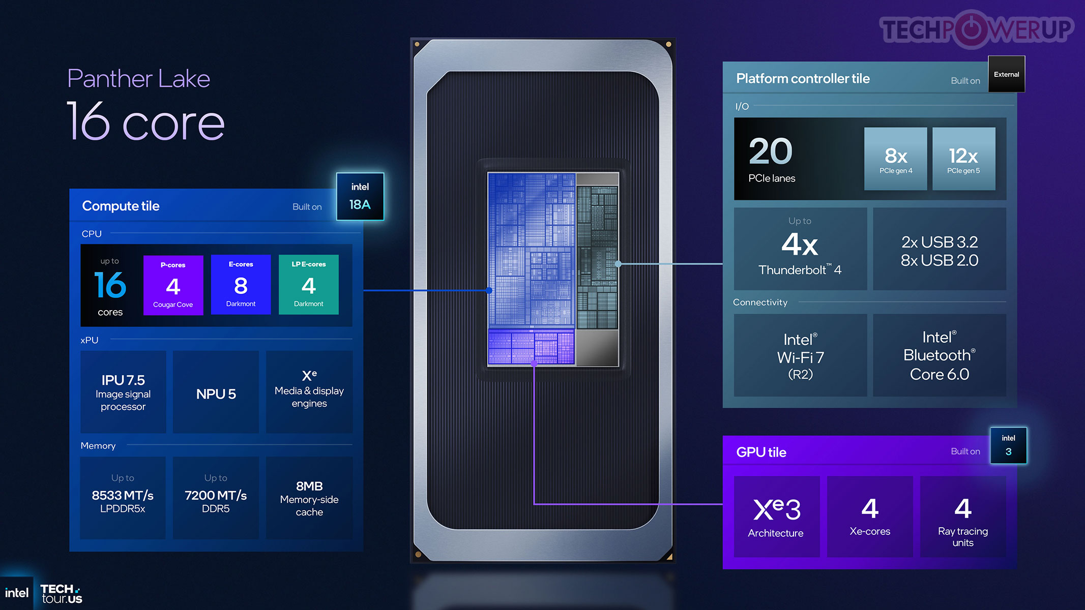

This slide shows the various package configurations of Panther Lake. As mentioned before, there are three variants: one eight-core, which is 4 P-Cores + 4 LP-E-Cores, combined with a small GPU tile with 4 Xe cores. The next variant is 4 P-Cores + 8 E-Cores + 4 LP-E-Cores, bringing the core count to 16. This is combined with the same small GPU tile, offering 4 Xe cores. Finally, we have the flagship version, which is the same CPU core config of 4x P + 8x E + 4x LP-E, but with a bigger GPU tile that offers 12 Xe Cores.
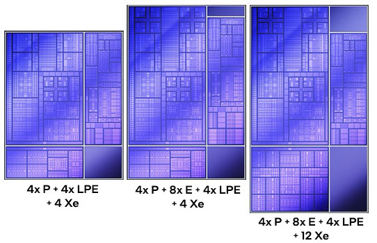
Here's another picture of the three die configs, which should help understand the differences. Note how from the first to the second, they are adding the E-Core cluster on top, and the bigger die on the right with the additional x8 PCIe lanes at the bottom, but the rest stays the same. Moving from second to third, we can see the much bigger GPU at the bottom, but the compute die stays the same, but the platform die is switched back to the smaller version that we saw on the left side, which lacks the additional 8 PCIe lanes. In the right corners, the dark rectangles are dummy dies without function that only serve to provide stability for the whole chip.

The graphics tile comes in two configurations: a smaller four-Xe-core design and a larger twelve-Xe-core version. The larger tile is built by TSMC, while the smaller tile is based on Intel 3 and targets lower-power systems.


Each Xe core includes updated vector and matrix engines, larger caches, and improved ray tracing units. Intel's data shows the twelve-Xe configuration delivering roughly twice the graphics performance of the Lunar Lake GPU at comparable power levels.

The platform controller tile, produced by TSMC, houses the PCI Express Gen 5 lanes, Thunderbolt interfaces, USB, and MACs for Bluetooth and wireless connectivity. The memory controller is located not here—it's inside the compute tile. It seems there are two different versions of the platform controller tile, with the second having an additional PCIe x8 5.0 interface for an external GPU (or they are using a single die with some parts disabled). The flexibility of this tile design allows Intel and OEMs to support a wide range of notebook classes from the same SoC family.
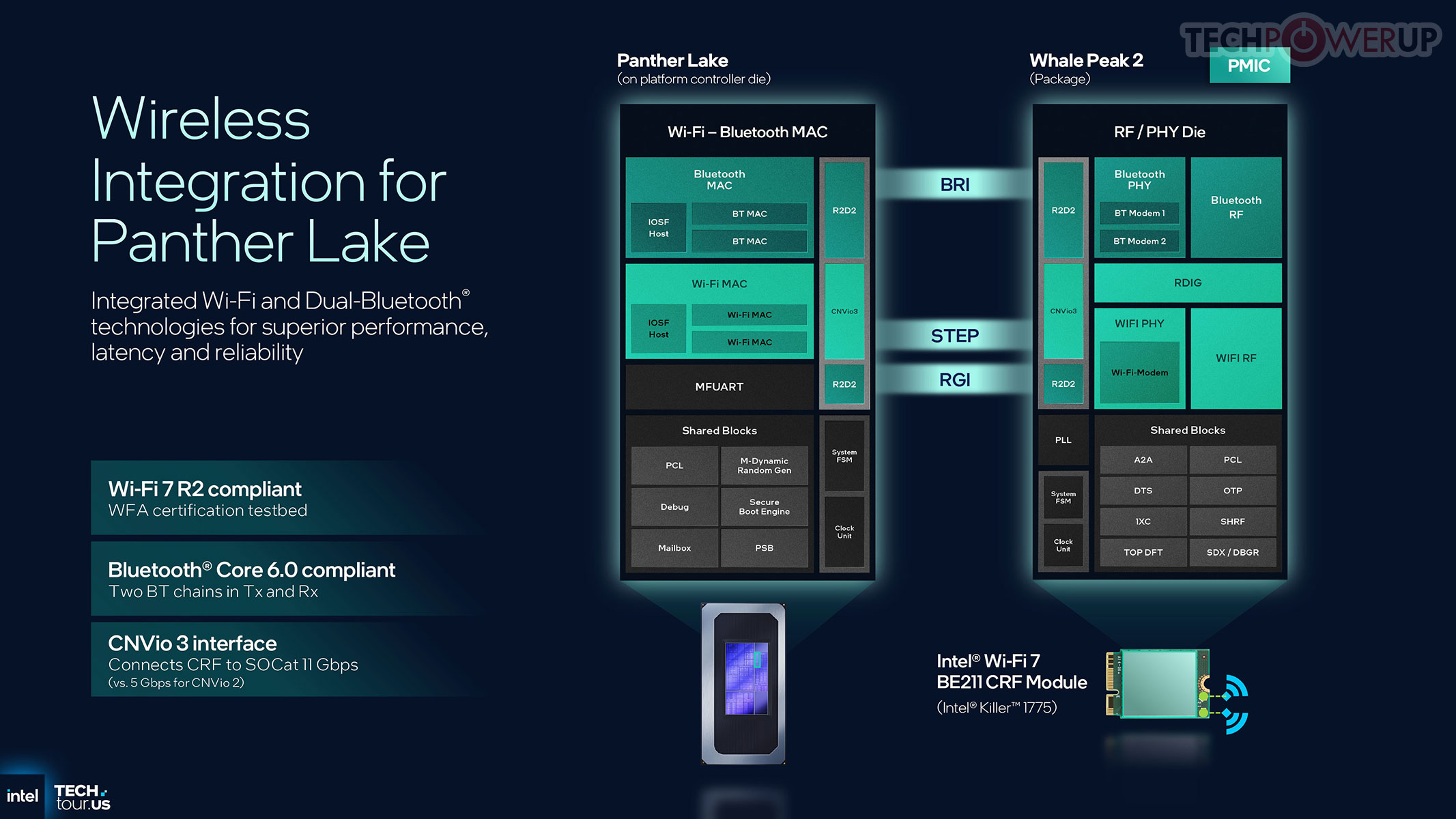
Just to expand on Bluetooth and Wi-Fi a bit. Here you can see a more detailed view that shows that the MACs for Bluetooth and Wi-Fi are in the platform controller die, i.e. "inside" the CPU, but the PHYs are located on a separate module called "Whale Peak 2." The MAC deals with how data is organized and transmitted, whereas the PHY handles the actual analog radio signal and antenna interfacing. This helps move the analog circuitry away from all the noise near the digital CPU die and offers more manufacturing flexibility.

By combining different tiles and core counts, Intel can scale Panther Lake from ultra-low-power devices to high-performance notebooks. Smaller designs will use the compact GPU tile and fewer active CPU cores, while larger configurations enable all core clusters and the full twelve-Xe GPU. This modular approach provides Intel with a single architecture that spans a wide range of power envelopes and product tiers.
Nov 18th, 2026 18:31 PST
change timezone
Latest GPU Drivers
New Forum Posts
- Dual B70 or Dual R9700 Pro on Linux (6)
- Time to upgrade CPU and MOBO (37)
- 26.11.2 Adrenalin Edition is out (0)
- Honestly, do you care about GTA VI? (149)
- Without Jensen, PC gaming will be (45)
- [Poll] 12V-2x6 Connector Protection: What Are You Using? (WireView / Ampinel / Equalizer / Other / Nothing) (42)
- Got a new laptop! What should I do with it? (6)
- What are you playing? (26235)
- Can i play GTA 6 now? (Joke) (8)
- Dell Workstation Owners Club (3514)
Popular Reviews
- Acemagic Retro X3 Review
- Upcoming Hardware Launches 2027 (Updated Nov 2026)
- AMD Zen 6 Technical Deep Dive
- Ugreen NASync DXP4800 GT Review
- Pulsar Office Tour & First Look at P1 Dual-Sensor Mouse
- Biwin Black Opal NV7400 2 TB Review
- Sapphire Radeon RX 7700 XT Pure Review
- Chieftec Iceberg PRO 360 DARK Review
- Sapphire Radeon RX 7700 XT Pulse Review
- ASUS ROG Strix B850-I Gaming Wi-Fi7 W Review
TPU on YouTube
Controversial News Posts
- NVIDIA Co-Founder and CEO Jensen Huang Officially Resigns (483)
- Report: Jensen Huang Eyes NVIDIA Comeback (196)
- Open Letter Asking NVIDIA to Reinstate Jensen Huang Passes 115,000 Signatures (184)
- OpenAI CEO Argues Home PCs Waste the World's Limited DRAM Supply (152)
- NVIDIA Launches Investigation Into Jensen Huang's Relationship With Suspected Chinese Spy (136)
- Intel "Raptor Lake Next" 16-Core and 20-Core CPUs Surface (130)
- Legendary Game Studio BioWare Shuts Down Following EA Layoffs (104)
- Dell CEO Says the Memory Shortage Will Get Worse in 2027 (95)