 0
0
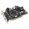
MSI N450GTS Cyclone OC 1 GB Review
Packaging & Contents »Introduction
Today NVIDIA launches their new GeForce GTS 450 Series of graphics cards. As the "GTS" naming suggests, the card is more of a mid-range part than a high-performance device. It is NVIDIA's expressed goal to offer a low priced DirectX 11 graphics card that the majority of gamers can afford - and still play the latest games.
Architecture

NVIDIA's GF106 GPU is based on NVIDIA's Fermi architecture, which was released earlier this year. In order to achieve the product performance and positioning NVIDIA was looking for, they disabled some components of the full GF106 core, resulting in the graphics processor for the GeForce GTS 450. Unlike other Fermi-class cards the changes here are quite limited. Basically NVIDIA removed two memory chips from the design, two chips less means 2x 32-bit less bus interface, so a single 64-bit memory controller got disabled. The memory bus width is closely coupled to the number of active ROPs in the GPU, so one ROP partition is also disabled. Overall this change enables board partners to build more price competitive products because of the reduced cost for memory chips and PCB signal routing. It helps NVIDIA to increase its GPU yields. This also leaves NVIDIA with the option to create a more powerful "GTS 455" SKU at a later time, that has a 192-bit GDDR5 memory interface, with likely 768 MB or 1536 MB of memory.
It's interesting to note that NVIDIA did not disable any of the streaming multiprocessor units (SMs), and all four SMs holding 48 CUDA cores each are enabled, giving the CUDA core count of 192. NVIDIA's reference clocks on the GeForce GTS 450 are fairly low with 783 MHz core, 1566 MHz CUDA cores, and 900 MHz memory, so it comes as no surprise that most board partners are shipping pre-overclocked cards at lauch.
MSI's GeForce GTS 450 uses a custom PCB design and MSI's well-established Cyclone thermal solution. The card comes with an overclock out of the box at 850 MHz core and 1000 MHz memory which is a bit lower than the average of factory overclocks on the GTS 450 models tested today.
| Radeon HD 4850 | GeForce GTS 250 | Radeon HD 5750 | GeForce GTS 450 | MSI GTS 450 Cyclone OC | Radeon HD 4870 | Radeon HD 5770 | GeForce | GeForce GTX 460 | Radeon HD 5830 | GeForce GTX 275 | GeForce GTX 460 | |
| Shader units | 800 | 128 | 720 | 192 | 192 | 800 | 800 | 216 | 336 | 1120 | 240 | 336 |
| ROPs | 16 | 16 | 16 | 16 | 16 | 16 | 16 | 28 | 24 | 16 | 28 | 32 |
| GPU | RV770 | G92 | Juniper | GF106 | GF106 | RV770 | Juniper | GT200 | GF104 | Cypress | GT200 | GF104 |
| Transistors | 956M | 754M | 1040M | 1170M | 1170M | 956M | 1040M | 1400M | 1950M | 2154M | 1404M | 1950M |
| Memory Size | 512 MB | 1024 MB | 1024 MB | 1024 MB | 1024 MB | 512 MB | 1024 MB | 896 MB | 768 MB | 1024 MB | 896 MB | 1024 MB |
| Memory Bus Width | 256 bit | 256 bit | 128 bit | 128 bit | 128 bit | 256 bit | 128 bit | 448 bit | 192 bit | 256 bit | 448 bit | 256 bit |
| Core Clock | 625 MHz | 738 MHz | 700 MHz | 783 MHz | 850 MHz | 750 MHz | 850 MHz | 576 MHz | 675 MHz | 800 MHz | 602 MHz | 675 MHz |
| Memory Clock | 993 MHz | 1100 MHz | 1150 MHz | 900 MHz | 1000 MHz | 900 MHz | 1200 MHz | 999 MHz | 900 MHz | 1000 MHz | 1107 MHz | 900 MHz |
| Price | $95 | $110 | $125 | $129 | $135 | $135 | $140 | $180 | $170 | $190 | $230 | $230 |
Apr 16th, 2024 13:28 EDT
change timezone
Latest GPU Drivers
New Forum Posts
- Cyberpunk 2077 Game Discussion (2119)
- Outer Worlds getting boring (22)
- Strange behaviour with my i5 1235u HP laptop after Windows reinstall (10)
- CPU exceeding maximum turbo speeds (6)
- NVCleanInstall Error: Access to the path ”DisplayDriverExt.dll” is denied. (5)
- Time to update the motherboards layout! (104)
- ThrottleStop Only Applying CPU Core Offset, NOT CPU Cache Offset (22)
- Free Games Thread (3752)
- Dell Workstation Owners Club (3048)
- The TPU Darkroom - Digital SLR and Photography Club (3946)
Popular Reviews
- Horizon Forbidden West Performance Benchmark Review - 30 GPUs Tested
- PowerColor Radeon RX 7900 GRE Hellhound Review
- Galax GeForce RTX 4070 Super EX Review
- Fractal Design Terra Review
- ASUS GeForce RTX 4090 Matrix Platinum Review - The RTX 4090 Ti
- Corsair 2000D Airflow Review
- Minisforum EliteMini UM780 XTX (AMD Ryzen 7 7840HS) Review
- Creative Pebble X Plus Review
- FiiO KB3 HiFi Mechanical Keyboard Review - Integrated DAC/Amp!
- ASUS GeForce RTX 4090 STRIX OC Review
Controversial News Posts
- NVIDIA Points Intel Raptor Lake CPU Users to Get Help from Intel Amid System Instability Issues (102)
- US Government Wants Nuclear Plants to Offload AI Data Center Expansion (98)
- Sony PlayStation 5 Pro Specifications Confirmed, Console Arrives Before Holidays (94)
- Developers of Outpost Infinity Siege Recommend Underclocking i9-13900K and i9-14900K for Stability on Machines with RTX 4090 (82)
- Windows 10 Security Updates to Cost $61 After 2025, $427 by 2028 (79)
- TechPowerUp Hiring: Reviewers Wanted for Motherboards, Laptops, Gaming Handhelds and Prebuilt Desktops (70)
- Intel Realizes the Only Way to Save x86 is to Democratize it, Reopens x86 IP Licensing (70)
- AMD Zen 5 Execution Engine Leaked, Features True 512-bit FPU (63)