 11
11
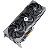
MSI GeForce RTX 5060 Ti Gaming Trio OC 16 GB Review
Neural Rendering, DLSS 4, Reflex 2 »NVIDIA Blackwell Architecture

NVIDIA does not provide a block diagram for the GB206 GPU (we asked), so we had to quickly hack one out from the GB202 diagram. This is accurate just not as pretty.
The GeForce Blackwell graphics architecture heralds NVIDIA's 4th generation of RTX, the late-2010s re-invention of the modern GPU that sees a fusion of real time ray traced objects with conventional raster 3D graphics. With Blackwell, NVIDIA is helping add another dimension, neural rendering, the ability for the GPU to leverage a generative AI to create portions of a frame. This is different from DLSS, where an AI model is used to reconstruct details in an upscaled frame based on its training date, temporal frames, and motion vectors. Today we are reviewing NVIDIA's fifth GPU from this generation, the RTX 5060 Ti. At the heart of this graphics card is the new GB206 silicon. This chip has a unique die-size and SM count that doesn't have a predecessor from the previous Ada generation. With the GeForce Blackwell generation, NVIDIA tailored the SM counts of its GPUs closer to those of the actual SKUs, to minimize wasted die-space. The GB206 is maxed out by the RTX 5060 Ti. This is NVIDIA's fourth gaming GPU based on this architecture. It is built on the same NVIDIA 4N foundry node as the previous generation AD106. It is a tiny, somewhat square die measuring 181 mm², with a transistor count of 21.9 billion.
The GB206 silicon is laid out essentially in the same component hierarchy as past generations of NVIDIA GPUs, but with a few notable changes. The GPU features a PCI-Express 5.0 x8 host interface. PCIe Gen 5 has been around since Intel's 12th Gen Core "Alder Lake" and AMD's Ryzen 7000 "Zen 4," so there is a sizable install-base of systems that can take advantage of it. The GPU is of course compatible with older generations of PCIe. The GB206 also features the new GDDR7 memory interface that's making its debut with this generation. The chip features a 128-bit wide memory bus. NVIDIA is using this to drive 16 GB of memory at 28 Gbps speeds, yielding 448 GB/s of memory bandwidth, which is a 55% increase over the RTX 4060 Ti and its 18 Gbps GDDR6.
The GigaThread Engine is the main graphics rendering workload allocation logic on the GB206, but there's a new addition, a dedicated serial processor for managing all AI acceleration resources on the GPU, NVIDIA calls this AMP (AI management processor). Other components at the global level are the Optical Flow Processor, a component involved in older versions of DLSS frame generation and for video encoding; and an updated media acceleration engine consisting of one each of NVDEC and NVENC video accelerators. The new 9th Gen NVENC video encode accelerators come with 4:2:2 AV1 and HEVC encoding support. The central region of the GPU has the single largest common component, the 32 MB L2 cache, which the RTX 5060 Ti maxes out.


There are three graphics processing clusters (GPC) on the GB206. Each of these contains 12 streaming multiprocessors (SM) across 6 texture processing clusters (TPCs), resulting in 36 SM. Every GPC also contains a ROP partition with 12 ROPs, each, working out to 48 ROPs on the silicon. Within each SM, you'll find 128 CUDA cores. Unlike the Ada generation SM that each had 64 FP32+INT32 and 64 purely-FP32 SIMD units, the new Blackwell generation SM features concurrent FP32+INT32 capability on all 128 SIMD units. These 128 CUDA cores are arranged in four slices, each with a register file, a level-0 instruction cache, a warp scheduler, two sets of load-store units, and a special function unit (SFU) handling some special math functions such as trigonometry, exponents, logarithms, reciprocals, and square-root. The four slices share a 128 KB L1 data cache, and four TMUs. The most exotic components of the Blackwell SM are the four 5th Gen Tensor cores, and a 4th Gen RT core.
With 3 GPCs containing 6 TPCs each, there are a total of 36 SM, worth 4,160 CUDA cores, 144 Tensor cores, 36 RT cores, and 144 TMUs, on the GB206 silicon. The GB206 silicon is endowed with 48 ROPs, all of which are enabled on the RTX 5060 Ti. The RTX 5060 Ti also maxes out all 32 MB of L2 cache present on the die.


Perhaps the biggest change to the way the SM handles work, introduced with Blackwell, is the concept of neural shaders—treating portions of the graphics rendering workload done by a generative AI model as shaders. Microsoft has laid the groundwork for standardization of neural shaders with its Cooperative Vectors API, in the latest update to DirectX 12. The Tensor cores are now accessible for workloads through neural shaders, and the shader execution reordering (SER) engine of the Blackwell SM is able to more accurately reorder workloads for the CUDA cores and the Tensor core in an SM.


The new 5th Gen Tensor core introduces support for FP4 data format (1/8 precision) to fast moving atomic workloads, providing 32 times the throughput of the very first Tensor core introduced with the Volta architecture. Over the generations, AI models leveraged lesser precision data formats, and sparsity, to improve performance. The AI management processor (AMP) is what enables simultaneous AI and graphics workloads at the highest levels of the GPU, so it could be simultaneously rendering real time graphics for a game, while running an LLM, without either affecting the performance of the other. AMP is a specialized hardware scheduler for all the AI acceleration resources on the silicon. This plays a crucial role for DLSS 4 multi-frame generation to work.


The 4th Gen RT core not just offers a generational increase in ray testing and ray intersection performance, which lowers the performance cost of enabling path tracing and ray traced effects; but also offers a potential generational leap in performance with the introduction of Mega Geometry. This allows for ray traced objects with extremely high polygon counts, increasing their detail. Poly count and ray tracing present linear increases in performance costs, as each triangle has to intersect with a ray, and there should be sufficient rays to intersect with each of them. This is achieved by adopting clusters of triangles in an object as first-class primitives, and cluster-level acceleration structures. The new RT cores introduce a component called a triangle cluster intersection engine, designed specifically for handling mega geometry. The integration of a triangle cluster compression format and a lossless decompression engine allows for more efficient processing of complex geometry.


The GB206 and the rest of the GeForce Blackwell GPU family is built on the exact same TSMC "NVIDIA 4N" foundry node, which is actually 5 nm, as previous-generation Ada, so NVIDIA directed efforts to finding innovative new ways to manage power and thermals. This is done through a re-architected power management engine that relies on clock gating, power gating, and rail gating of the individual GPCs and other top-level components. It also worked on the speed at which the GPU makes power-related decisions.

The quickest way to drop power is by adjusting the GPU clock speed, and with Blackwell, NVIDIA introduced a means for rapid clock adjustments at the SM-level.

NVIDIA updated both the display engine and the media engine of Blackwell over the previous generation Ada, which drew some flack for holding on to older display I/O standards such as DisplayPort 1.4, while AMD and Intel had moved on to DisplayPort 2.1. The good news is that Blackwell supports DP 2.1 with UHBR20, enabling 8K 60 Hz with a single cable. The company also updated NVDEC and NVENC, which now support AV1 UHQ, double the H.264 decode performance, MV-HEVC, and 4:2:2 formats.
Apr 25th, 2025 00:07 EDT
change timezone
Latest GPU Drivers
New Forum Posts
- Cracks in my cpu waterblock should I be concerned? (13)
- What's your latest tech purchase? (23595)
- Have you got pie today? (16677)
- Are the 8 GB cards worth it? (177)
- pc randomly blackscreening (0)
- What are you playing? (23462)
- I dont understand the phone OS world..... (49)
- New OLED monitor makes PC unresponsive sometimes (28)
- RTX 5070ti - Which MSRP model has the better/quieter cooler design, ASUS Prime, Gigabyte Windforce or PNY? (7)
- I tried to use AMD Auto Overclock, and now my PC has been freezing up sometimes. Afterwards, the screen goes black or displays artifacts. (29)
Popular Reviews
- NVIDIA GeForce RTX 5060 Ti 8 GB Review - So Many Compromises
- Crucial CUDIMM DDR5-6400 128 GB CL52 Review
- Colorful iGame B860M Ultra V20 Review
- ASUS GeForce RTX 5060 Ti TUF OC 16 GB Review
- Upcoming Hardware Launches 2025 (Updated Apr 2025)
- Sapphire Radeon RX 9070 XT Pulse Review
- Sapphire Radeon RX 9070 XT Nitro+ Review - Beating NVIDIA
- ASRock X870E Taichi Lite Review
- AMD Ryzen 7 9800X3D Review - The Best Gaming Processor
- ASUS GeForce RTX 5080 TUF OC Review
Controversial News Posts
- NVIDIA GeForce RTX 5060 Ti 16 GB SKU Likely Launching at $499, According to Supply Chain Leak (182)
- NVIDIA Sends MSRP Numbers to Partners: GeForce RTX 5060 Ti 8 GB at $379, RTX 5060 Ti 16 GB at $429 (127)
- NVIDIA Launches GeForce RTX 5060 Series, Beginning with RTX 5060 Ti This Week (115)
- Nintendo Confirms That Switch 2 Joy-Cons Will Not Utilize Hall Effect Stick Technology (105)
- Nintendo Switch 2 Launches June 5 at $449.99 with New Hardware and Games (99)
- Sony Increases the PS5 Pricing in EMEA and ANZ by Around 25 Percent (84)
- NVIDIA PhysX and Flow Made Fully Open-Source (77)
- Windows Notepad Gets Microsoft Copilot Integration (75)