 49
MSI GeForce RTX 5080 Expert OC Review
(49 Comments) »Introduction

MSI GeForce RTX 5080 Expert OC is a premium custom design RTX 5080 graphics card by MSI that targets creators and content professionals primarily, and gamers that want a graphics card with a mature-looking design in their builds. It is also an attempt by the company to level up to the artistic finesse of NVIDIA's first-party Founders Edition. MSI launched Expert-series graphics cards based on the GeForce RTX 5080 and the RTX 5070 Ti just a few days ago, with regular and OC variants. In this review, we take the top RTX 5080 Expert OC for a spin.
MSI debuted the Expert line of graphics cards with the previous generation RTX 4080 Super and RTX 4070 Ti Super, and tried to replicate the dual-axial flow-through cooler design of the RTX 40-series Founders Edition graphics cards. We reviewed the RTX 4080 Super Expert, but were left disappointed, as the card offered close to no performance uplift over the Founders Edition card, and had the weakest cooling solution. MSI likely put great effort into redesigning its RTX 50-series Expert graphics cards without losing out on the core design language that defines Expert—high build quality, premium and sophisticated looks, and MSI's own take on dual-axial flow-through. The Expert series is part of MSI's two-pronged approach to exceeding the standards set by Founders Edition cards. The Expert series targets creators that game on the side, while the SUPRIM series targets enthusiast gamers. Creators can pair the MSI RTX 5080 Expert OC with NVIDIA's GeForce Studio drivers that are optimized for a number of content creation productivity suites.

The GeForce RTX 5080 is a powerful enthusiast-segment GPU that's next only to the flagship RTX 5090. It is designed for maxed out gameplay at 4K Ultra HD resolution, including with ray tracing, and the new DLSS 4 with Multi Frame Generation enabling newer experiences, such as 4K high refresh-rate. The RTX 5080 is powered by the Blackwell graphics architecture, which introduces Neural Rendering, a potentially revolutionary concept in consumer 3D graphics, which leverages generative AI models to create photorealistic objects that are combined with raster 3D graphics the same way ray traced objects are. DLSS 4 sees NVIDIA replace the convoluted neural network (CNN) based AI models driving the upscaling, ray-reconstruction, and frame-generation features with newer transformer based models that are more accurate and improve image quality at every performance tier. Multi Frame Generation lets up to 3 frames following every conventionally rendered frame to be drawn by AI, effectively quadrupling frame-rates and reducing CPU requirements of high refresh rate gaming.
With Blackwell, NVIDIA has improved every key component of the GPU over the previous Ada Lovelace architecture, which is important given that the company is building these chips on the same NVIDIA 4N foundry node. The new Blackwell CUDA cores not just introduce generational IPC increases, but are also redesigned to accelerate neural shaders. The 4th generation RT core, besides lowering the performance cost of ray tracing, comes with optimization for mega geometry—ray traced objects with much more complex geometry (more surfaces for rays to interact with). The 5th generation Tensor cores lay the groundwork for not just for neural rendering, but also introduce support for newer data formats, including FP4.
The GeForce RTX 5080 is based on the GB203 silicon, which it maxes out, enabling all 84 streaming multiprocessors (SM) physically present on the chip. It also comes with 16 GB of 30 Gbps GDDR7 memory across the chip's full 256-bit wide memory bus, for 960 GB/s of memory bandwidth. With 84 SM, the RTX 5080 gets 10,752 CUDA cores, 336 Tensor cores, 84 RT cores, 336 TMU, and the chip's full complement of 112 ROPs. NVIDIA also took the opportunity to modernize the display controllers of the GPU to support the latest DisplayPort 2.1 with UHBR20 and HDMI 2.1 standards; and updated the video encode and decode acceleration engines.
MSI has boosted the GeForce RTX 5080 Expert OC factory overclocked speeds to 2715 MHz boost compared to 2617 MHz on the reference, while leaving the memory untouched at 30 Gbps (GDDR7 effective). The company has given this card the same marquee as its MSI PRO range of commercial notebooks and desktops targeting creators and businesses. The MSI RTX 5080 Expert OC is priced at $1300 in the United States, but in Europe you can find it for the equivalent of $1100.
| Price | Cores | ROPs | Core Clock | Boost Clock | Memory Clock | GPU | Transistors | Memory | |
|---|---|---|---|---|---|---|---|---|---|
| RTX 4070 Super | $600 | 7168 | 80 | 1980 MHz | 2475 MHz | 1313 MHz | AD104 | 35800M | 12 GB, GDDR6X, 192-bit |
| RX 7900 GRE | $550 | 5120 | 160 | 1880 MHz | 2245 MHz | 2250 MHz | Navi 31 | 57700M | 16 GB, GDDR6, 256-bit |
| RTX 4070 Ti | $700 | 7680 | 80 | 2310 MHz | 2610 MHz | 1313 MHz | AD104 | 35800M | 12 GB, GDDR6X, 192-bit |
| RTX 5070 | $550 | 6144 | 80 | 2325 MHz | 2512 MHz | 1750 MHz | GB205 | 31100M | 12 GB, GDDR7, 192-bit |
| RTX 4070 Ti Super | $750 | 8448 | 96 | 2340 MHz | 2610 MHz | 1313 MHz | AD103 | 45900M | 16 GB, GDDR6X, 256-bit |
| RX 7900 XT | $620 | 5376 | 192 | 2000 MHz | 2400 MHz | 2500 MHz | Navi 31 | 57700M | 20 GB, GDDR6, 320-bit |
| RX 9070 | $550 | 3584 | 128 | 2070 MHz | 2520 MHz | 2518 MHz | Navi 48 | 53900M | 16 GB, GDDR6, 256-bit |
| RX 9070 XT | $615 | 4096 | 128 | 2400 MHz | 2970 MHz | 2518 MHz | Navi 48 | 53900M | 16 GB, GDDR6, 256-bit |
| RTX 5070 Ti | $750 | 8960 | 96 | 2295 MHz | 2452 MHz | 1750 MHz | GB203 | 45600M | 16 GB, GDDR7, 256-bit |
| RX 7900 XTX | $750 | 6144 | 192 | 2300 MHz | 2500 MHz | 2500 MHz | Navi 31 | 57700M | 24 GB, GDDR6, 384-bit |
| RTX 4080 | $850 | 9728 | 112 | 2205 MHz | 2505 MHz | 1400 MHz | AD103 | 45900M | 16 GB, GDDR6X, 256-bit |
| RTX 4080 Super | $1000 | 10240 | 112 | 2295 MHz | 2550 MHz | 1438 MHz | AD103 | 45900M | 16 GB, GDDR6X, 256-bit |
| RTX 5080 | $1000 | 10752 | 112 | 2295 MHz | 2617 MHz | 1875 MHz | GB203 | 45600M | 16 GB, GDDR7, 256-bit |
| MSI RTX 5080 Expert OC | $1100 | 10752 | 112 | 2295 MHz | 2715 MHz | 1875 MHz | GB203 | 45600M | 16 GB, GDDR7, 256-bit |
| RTX 4090 | $1800 | 16384 | 176 | 2235 MHz | 2520 MHz | 1313 MHz | AD102 | 76300M | 24 GB, GDDR6X, 384-bit |
| RTX 5090 | $2200 | 21760 | 176 | 2017 MHz | 2407 MHz | 1750 MHz | GB202 | 92200M | 32 GB, GDDR7, 512-bit |
Packaging
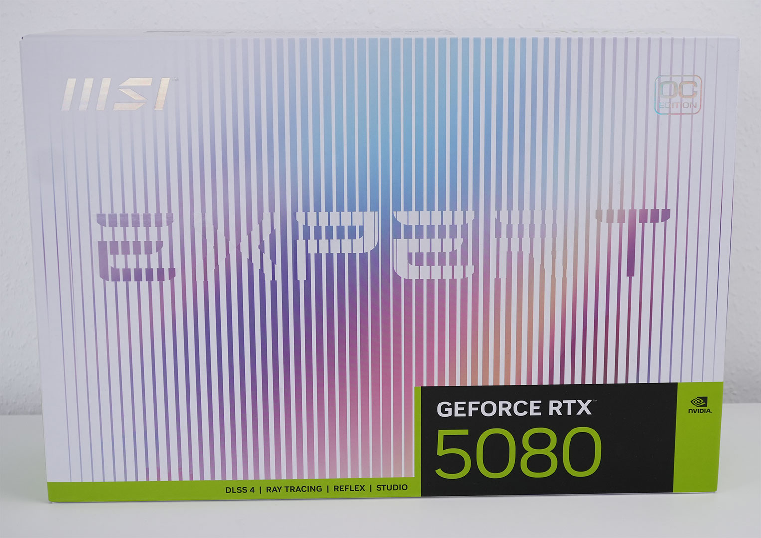
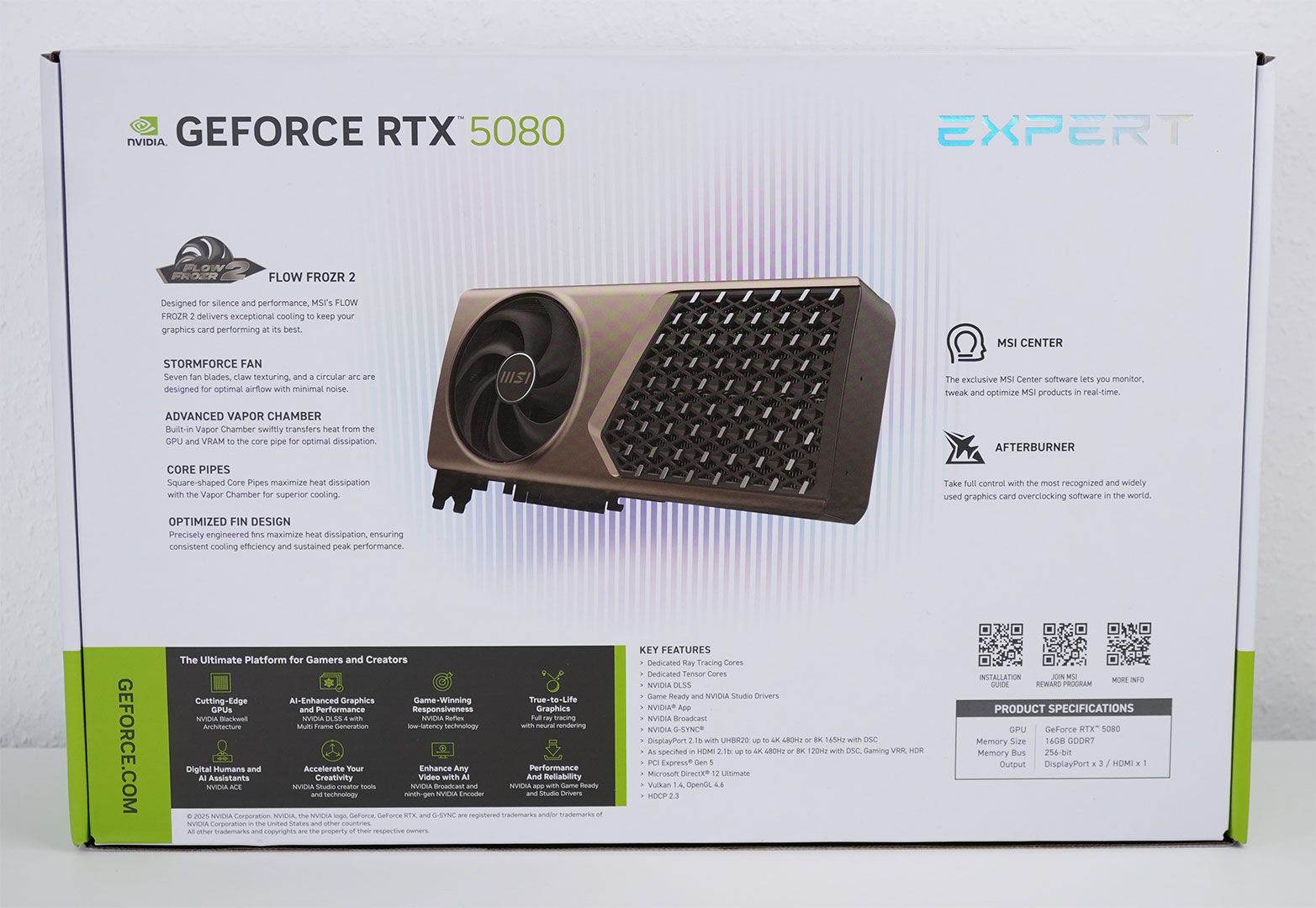
The Card


MSI has refreshed their Expert theme slightly, it looks extremely nice. Both the main cooler shroud and the backplate are made from high-quality metal with a nice matte gold surface texture. The cooler is designed so that hot air gets exhausted out of the card by the back fan and the front fan pulls air through the card.


Dimensions of the card are 32.0 x 15.0 cm, and it weighs 1885 g.
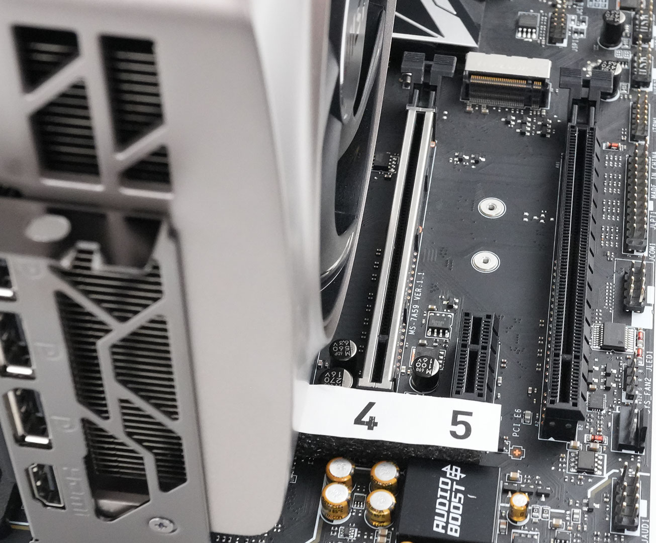

Installation requires three slots in your system. We measured the card's width to be 58 mm.
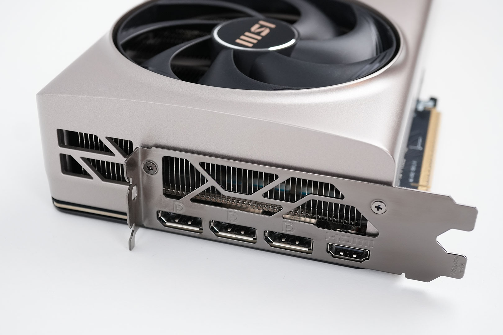
Display connectivity includes three standard DisplayPort 2.1b and one HDMI 2.1b.
All GeForce RTX 50-series Blackwell cards feature a new display engine supporting DisplayPort 2.1b with UHBR20, as well as HDMI 2.1a. Both interfaces support DSC (display stream compression). With DSC enabled, a single DisplayPort on this card can drive 4K 12-bit HDR at 480 Hz; or 8K 12-bit HDR at up to 165 Hz. The RTX 5080 features an updated media acceleration engine with support for 4:2:2 video formats, AV1 UHQ, and MV-HEVC. There are two independent NVENC and NVDEC units.
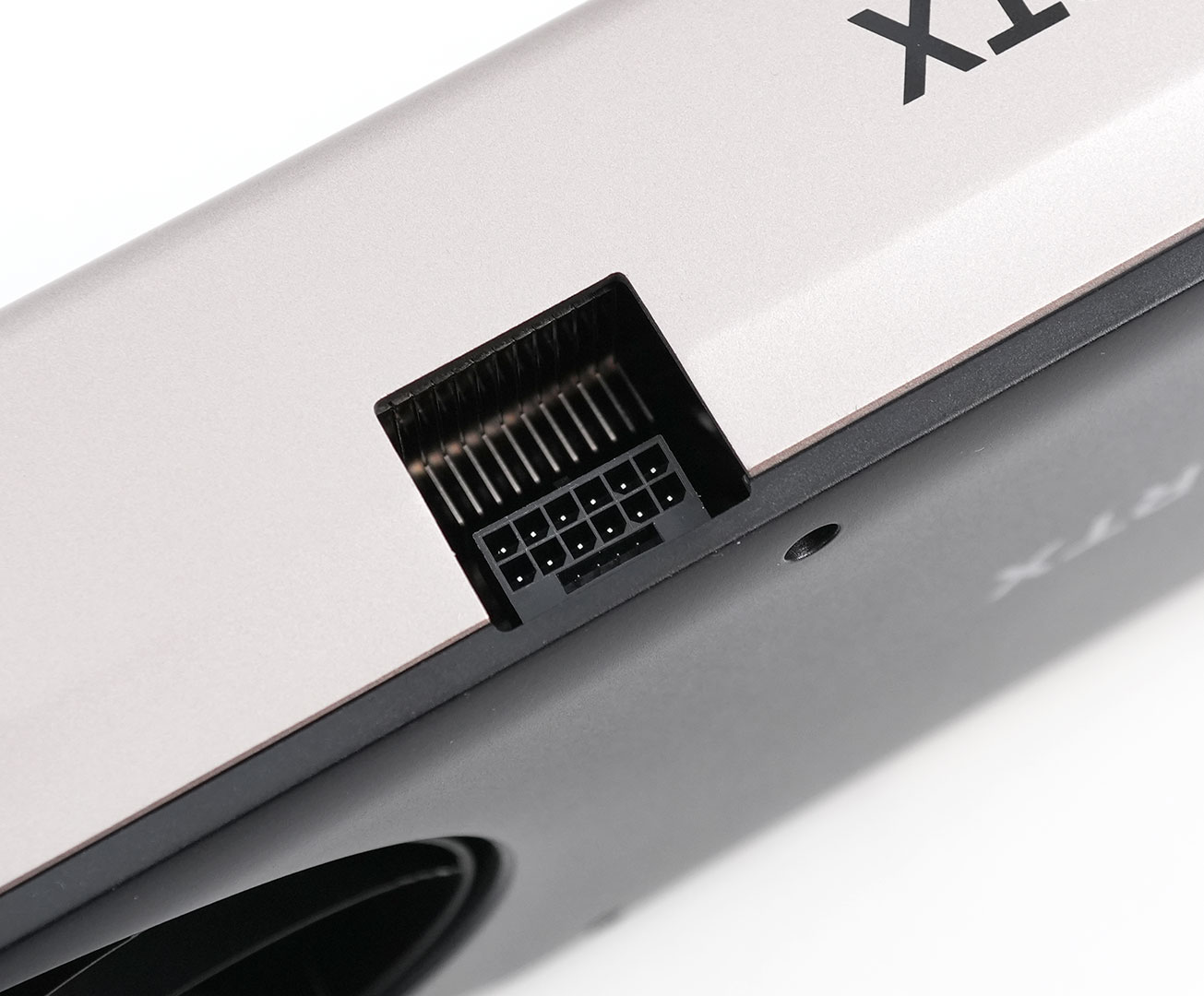
The card uses a single 16-pin connector, which allows a maximum power draw of 600 W, but the board power limit is set much lower of course, at 360 W, with a manual adjustment range allowing up to 400 W.

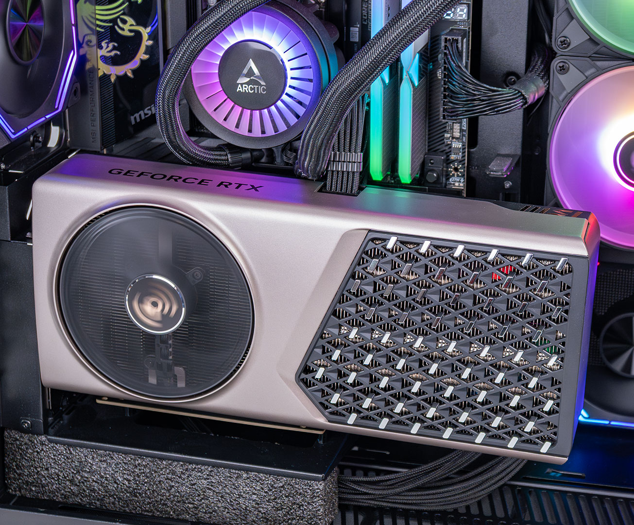
There is no lighting on the MSI RTX 5080 Expert.
Teardown

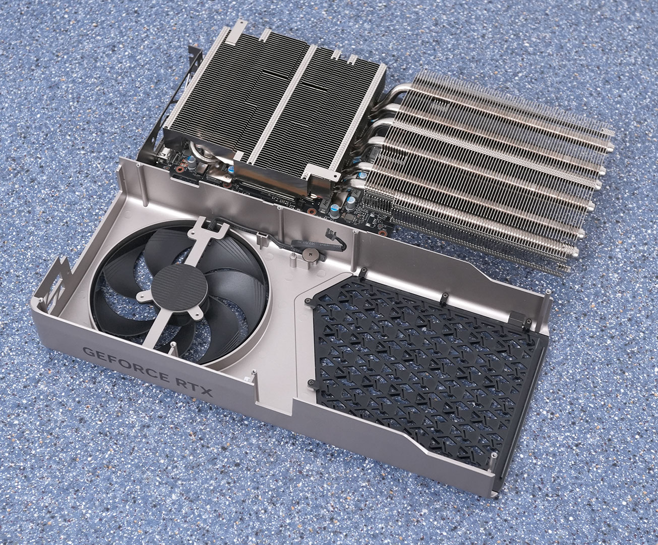
The card consists of three main pieces. The front golden cooler shroud, the PCB and heatsink assembly in the middle, and the black backplate. You can remove both outer components while the main heatsink remains in place—this is great for maintenance.
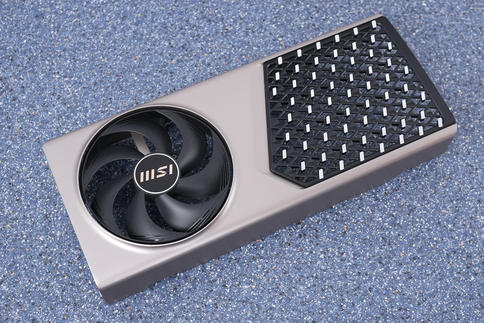
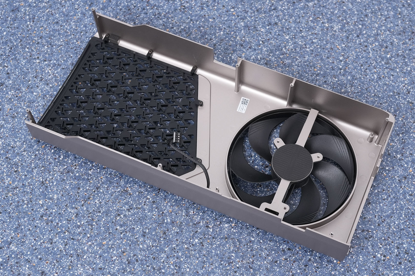
MSI's cooler shroud is made from metal and looks fantastic. I like the subtle details and robust build, which makes the card feel nearly indestructible.
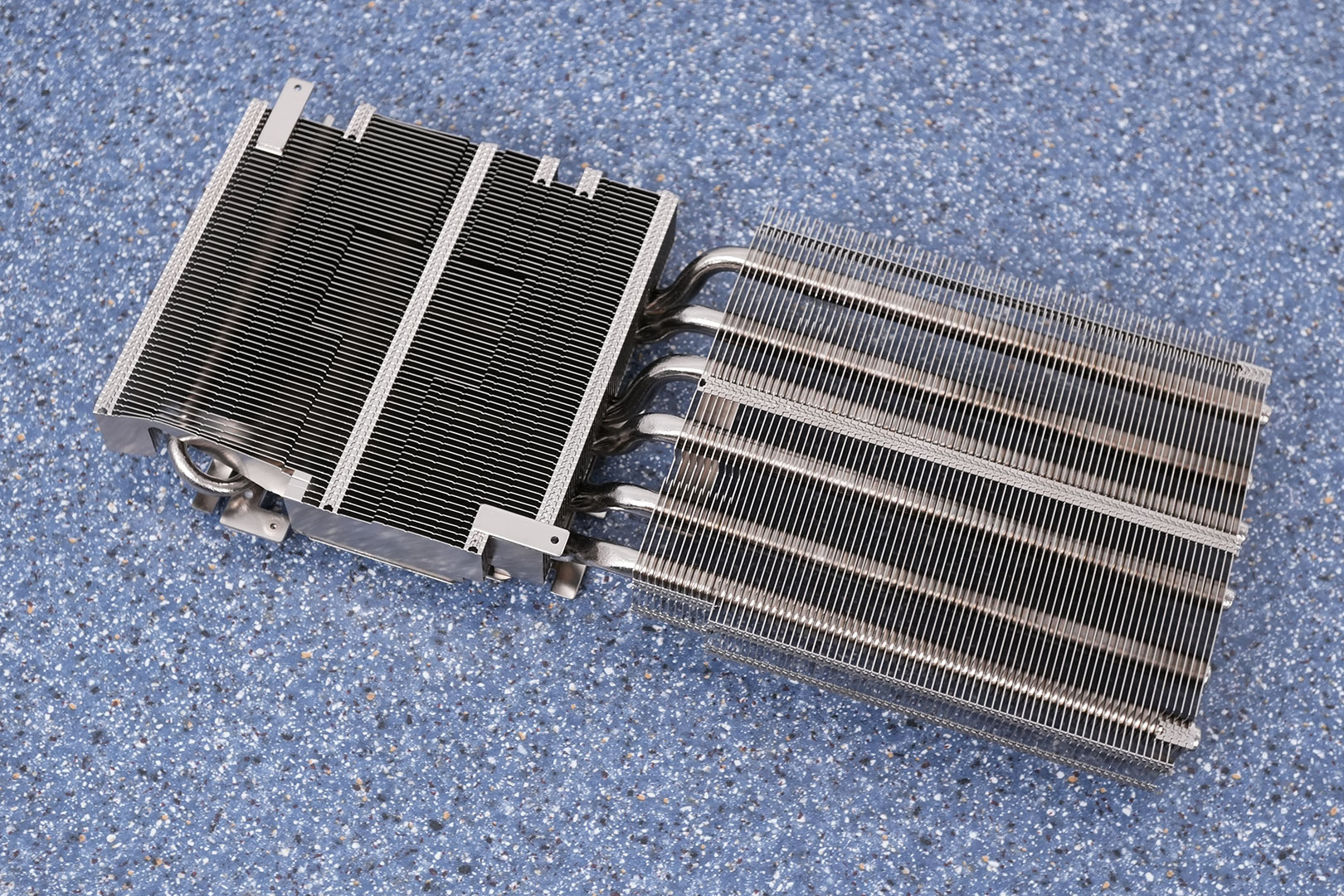


MSI's thermal solution uses seven heatpipes and a vapor-chamber (the seventh heatpipe is a short one that goes towards the left on the second picture above. The heatsink assembly provides cooling not only for the GPU, but also for the memory chips and VRM circuitry.
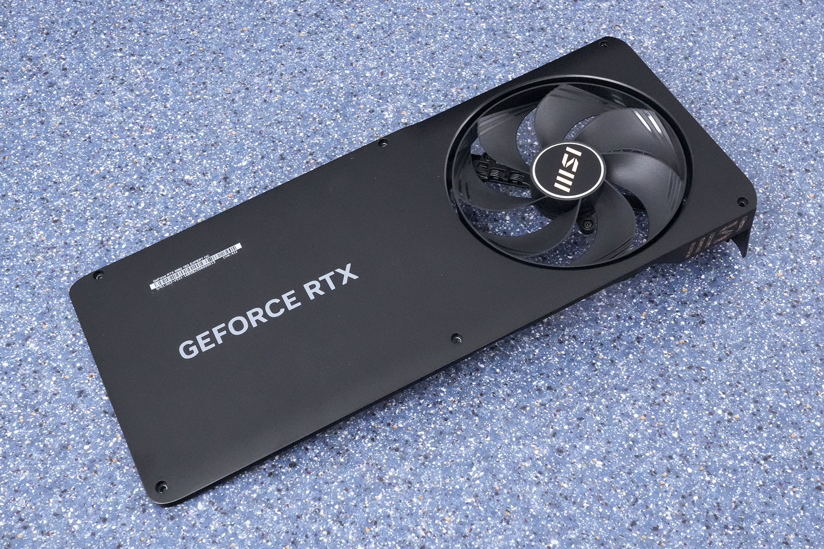
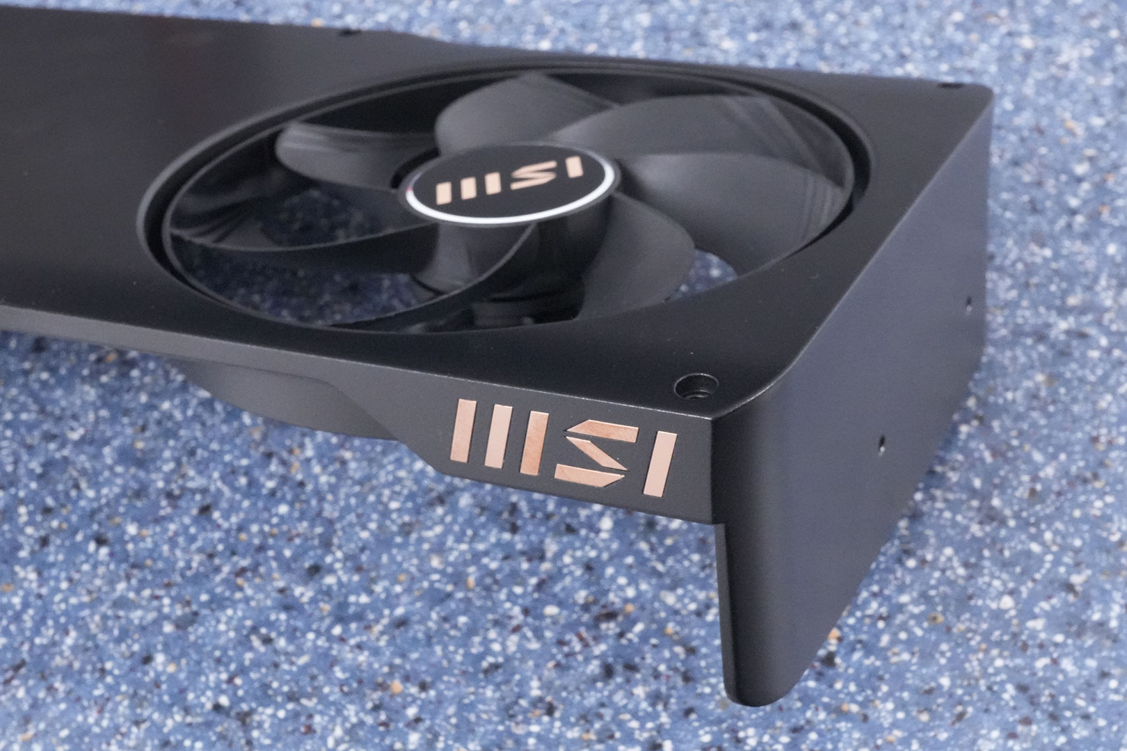
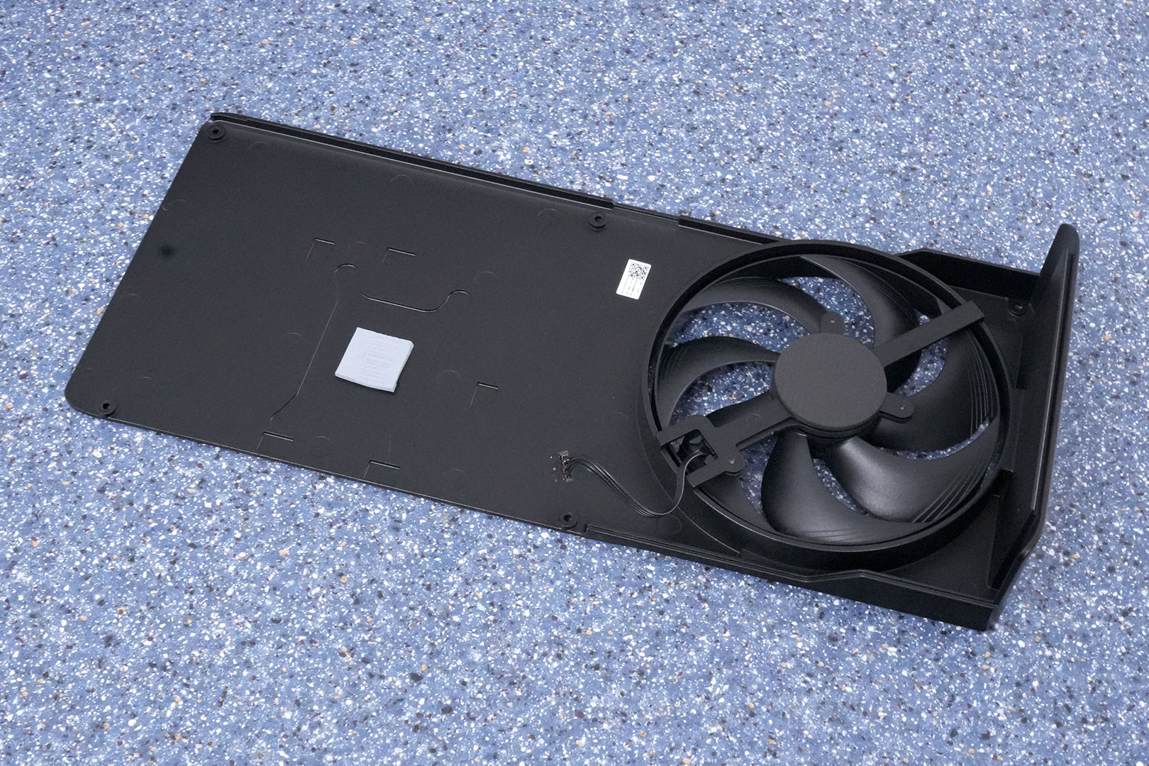
The backplate is built from thick metal, too, like the cooler shroud. It protects against damage during installation and handling.
High-resolution PCB Pictures
These pictures are for the convenience of volt modders and people who would like to see all the finer details on the PCB. Feel free to link back to us and use these in your articles, videos or forum posts.

High-resolution versions are also available (front, back).
Circuit Board (PCB) Analysis


A 15-phase VRM powers the GPU, highlighted in the red rectangles above. These are controlled by a Monolithic Power Systems MP29816 controller.

All GPU power phases use Monolithic MPS MP87993 DrMOS with a rating of 50 A.

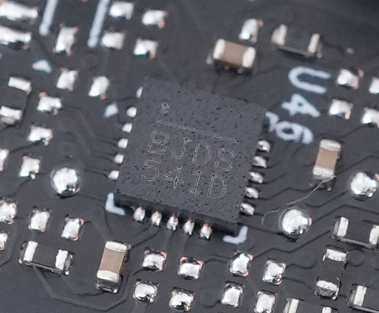
Powering the eight GDDR7 memory chips is a 3-phase VRM driven by a Monolithic MP2988 controller (this variant uses a smaller package).

Just like GPU, the memory is handled by Monolithic MP87993 DrMOS chips.

The GDDR7 memory chips are made by Samsung, and bear the model number K4VAF325ZC-SC32, they are rated for 32 Gbps.
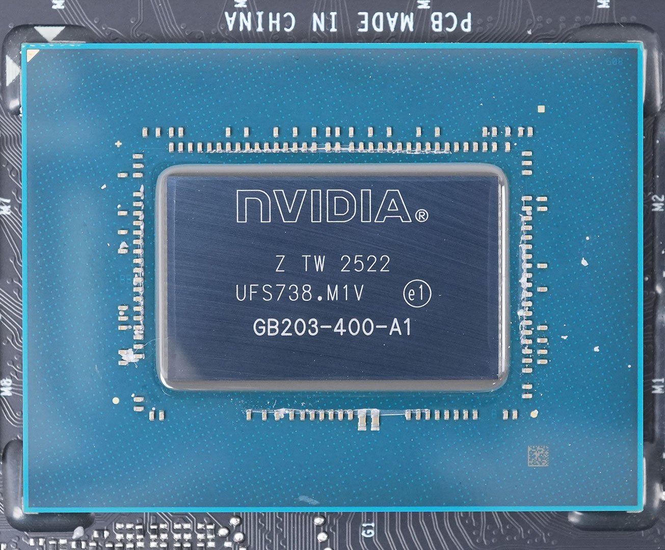
The NVIDIA GB203 GPU at the heart of the GeForce RTX 5080 is much smaller than the chip used on the RTX 5090. It is fabricated using a 5 nanometer "NVIDIA 4N" process at TSMC Taiwan (same process as Ada). The die measures 378 mm², and comes with a transistor count of 45.6 billion.
Test System
| Test System - GPU 2025.2 | |
|---|---|
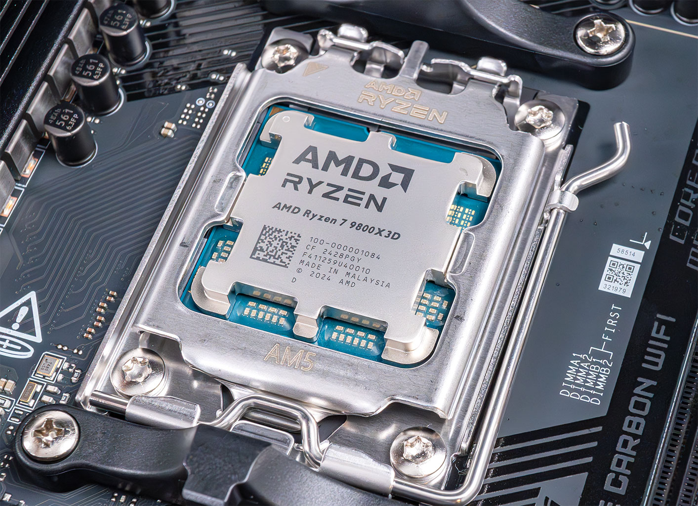
| Processor: | AMD Ryzen 7 9800X3D Zen 5, 5.2 GHz, 8 cores / 16 threads |
| Motherboard: | MSI X870E Carbon Wi-Fi BIOS 7E49v1A3 |
| Resizable BAR: | Enabled on all supported cards (NVIDIA, AMD & Intel) |
| Memory: | Thermaltake TOUGHRAM XG 2x 16 GB DDR5-6200 28-36-36-76 UCLK 1:1 |
| Cooling: | Arctic Liquid Freezer III 280 mm AIO |
| Thermal Paste: | Arctic MX-6 |
| Storage: | 4 TB M.2 NVMe SSD |
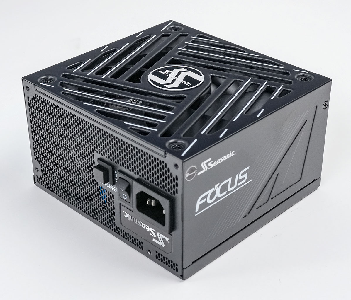
| Power Supply: | Seasonic Focus GX 1000 W ATX 3.0 / 16-pin 12VHPWR |
| Case: | darkFlash DY470 |
| Operating System: | Windows 11 Professional 64-bit 24H2 VBS enabled (Windows 11 default) |
| Drivers: | RTX 5050: 576.88 WHQL RTX 5060: 576.52 WHQL RTX 5060 Ti: 575.94 Press Driver Other NVIDIA cards: 572.83 WHQL RX 9070 XT & RX 9060 XT: 25.8.1 WHQL Other AMD cards: 25.3.2 Beta Intel: 101.6732 Beta Date of Retest |
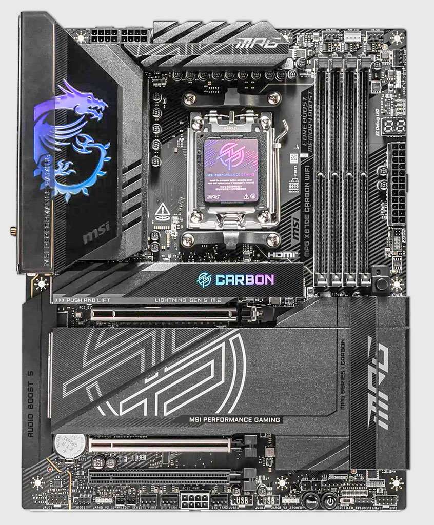
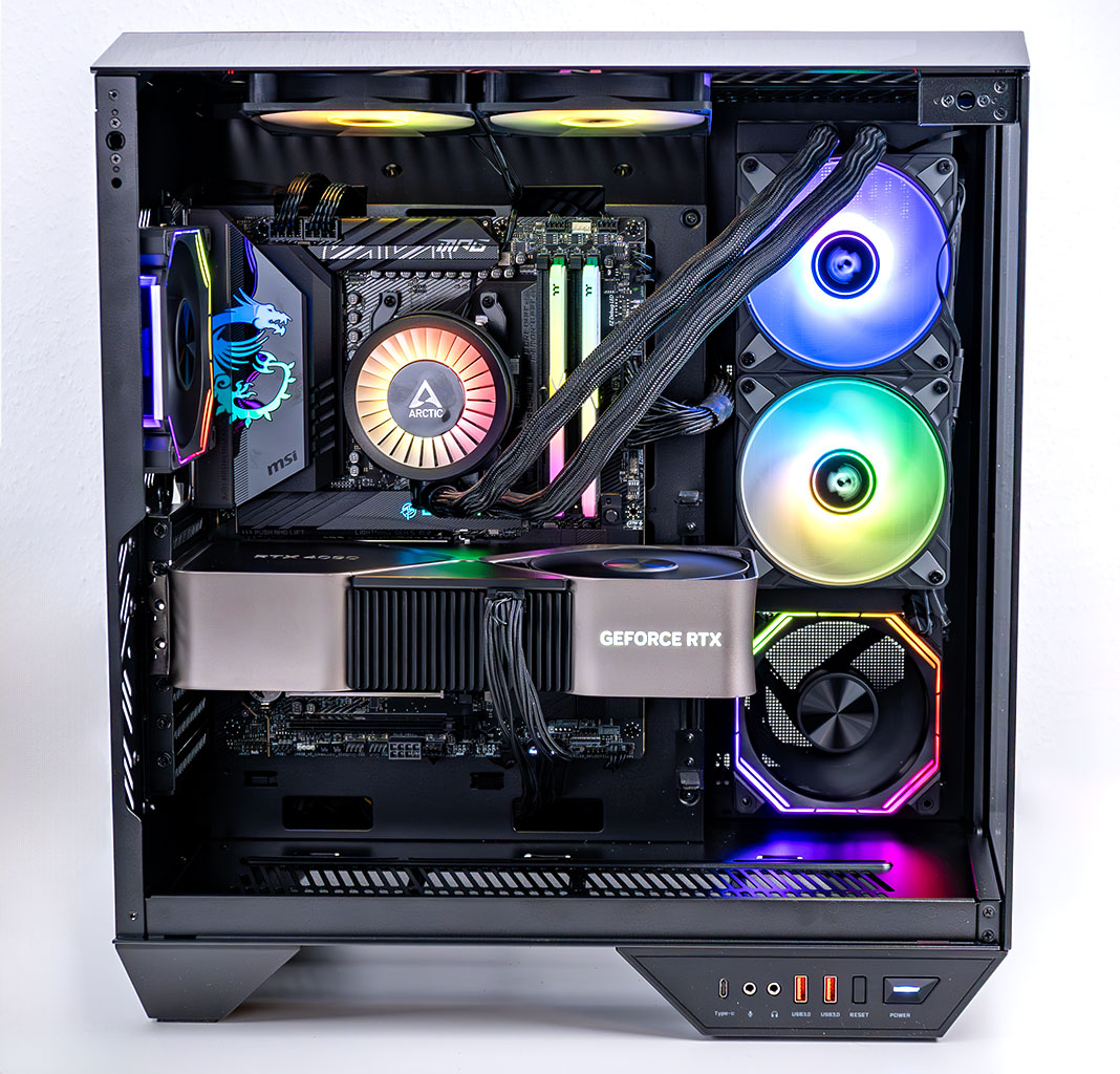
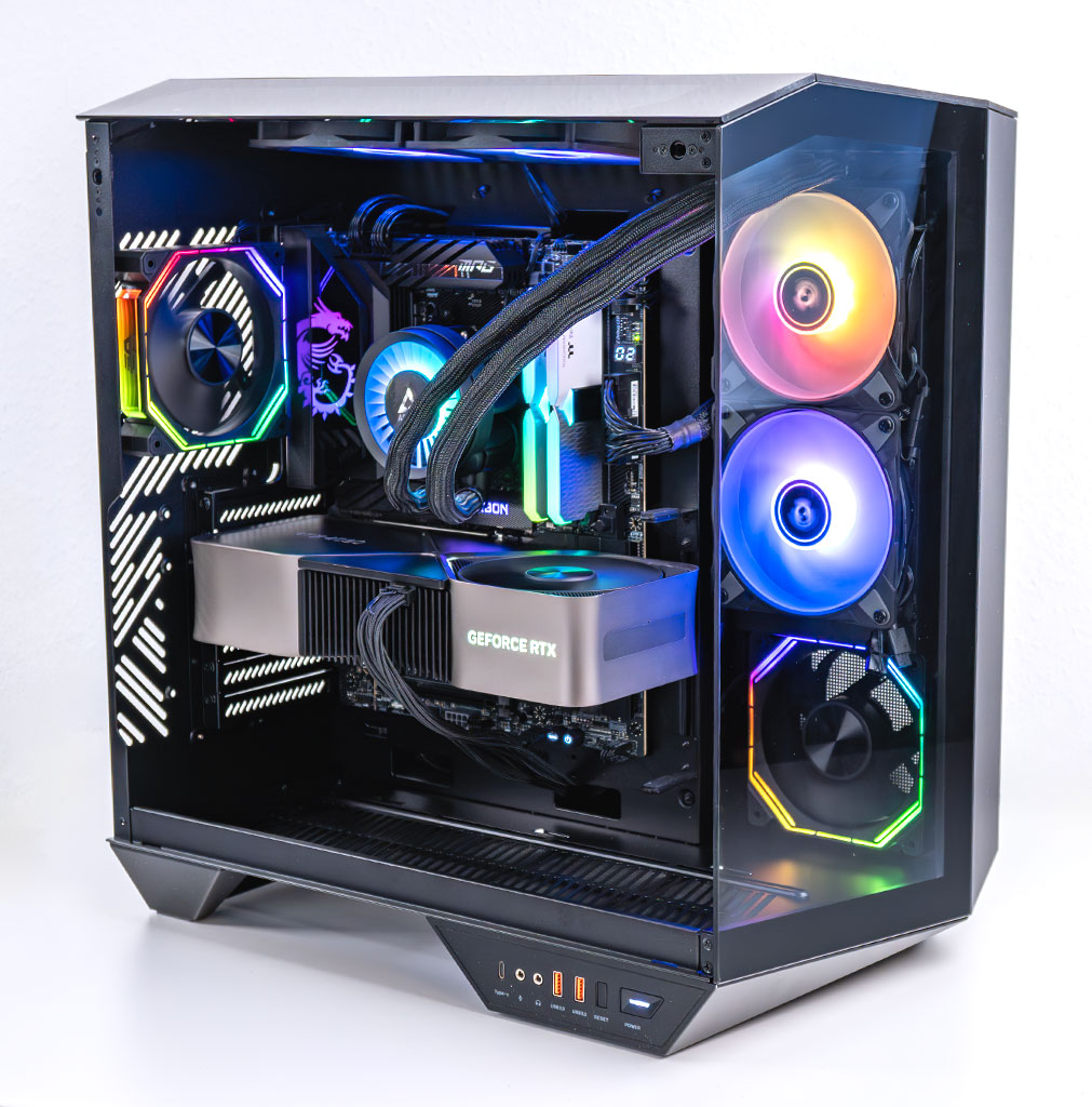
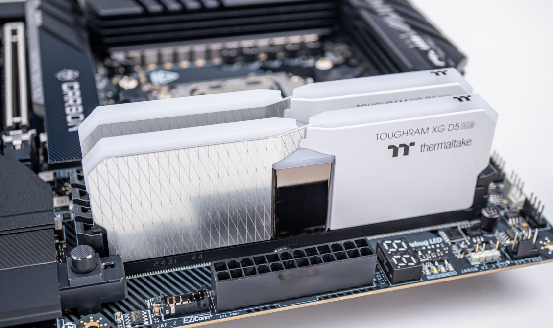

- All games and cards are tested with the drivers listed above—no performance results were recycled between test systems. Only this exact system with exactly the same configuration is used for all results in this review.
- All graphics cards are tested using the same game version.
- All games are set to their highest quality setting unless indicated otherwise.
- All games are running at their native resolution without upscaling (no DLSS or FSR), except for the results on the "DLSS 4" page where we specifically look into that feature's performance
- All games have ray tracing disabled, except for testing on the "Ray Tracing" and "Path Tracing" pages
- AA and AF are applied via in-game settings, not via the driver's control panel.
- Before starting measurements, we heat up the card for each test to ensure a steady state is tested. This ensures that the card won't boost to unrealistically high clocks for only a few seconds until it heats up, as that doesn't represent prolonged gameplay.
- For better real-life applicability, all game tests use custom in-game test scenes, not the integrated benchmarks
- All cards used for comparison are reference designs. When a reference design does not exist, we go the extra mile and buy the closest possible match, which has reference clocks and default power limit.
- 1920x1080: Most popular monitor resolution.
- 2560x1440: Intermediary resolution between Full HD and 4K, with reasonable performance requirements.
- 3840x2160: 4K Ultra HD resolution, available on high-end monitors.
Our Patreon Silver Supporters can read articles in single-page format.
Nov 14th, 2026 18:54 CST
change timezone
Latest GPU Drivers
New Forum Posts
- Honestly, do you care about GTA VI? (13)
- What is in your fleet, size and contents? (28)
- WarpCoreBench scores! (33)
- 9070 GRE 3.9ghz validation reached. (10)
- X79 and/or rampage IV OC'ing thread for those of us still left.... (2452)
- Can you guess Which game it is? (317)
- What can the FX 8320 do today? Here is the answer. (43)
- Ryzen 7 8700G OC (8)
- auto-closed by somethings by actions (2)
- [Community Benchmark] MrH OpenCL Benchmark 2.0e (Windows Only – CPU & GPU) (2)
Popular Reviews
- AMD Zen 6 Technical Deep Dive
- ASUS ROG Strix B850-I Gaming Wi-Fi7 W Review
- Corsair HX1000i Shift Crystal Review
- Upcoming Hardware Launches 2027 (Updated Nov 2026)
- Montech King 95 3D PRO Review
- NZXT C1200 Platinum Review
- NZXT H7 RGB+ Review
- NZXT H5 Review
- Phantom Blade Zero Performance Benchmark Review - 35 GPUs Tested
- AMD Ryzen 7 9800X3D Review - The Best Gaming Processor
TPU on YouTube
Controversial News Posts
- NVIDIA Co-Founder and CEO Jensen Huang Officially Resigns (406)
- OpenAI CEO Argues Home PCs Waste the World's Limited DRAM Supply (152)
- NVIDIA Launches Investigation Into Jensen Huang's Relationship With Suspected Chinese Spy (136)
- Intel "Raptor Lake Next" 16-Core and 20-Core CPUs Surface (130)
- Legendary Game Studio BioWare Shuts Down Following EA Layoffs (104)
- Dell CEO Says the Memory Shortage Will Get Worse in 2027 (95)
- NVIDIA GeForce RTX 50-Series Scheduled for up to $500 Price Hike This Week (89)
- Modder Fits RTX 5090 With Four 8-Pin Connectors, Halving Current per Wire (80)