 97
97
Sapphire Radeon RX 7900 GRE Pulse Review
(97 Comments) »Introduction
AMD Radeon RX 7900 GRE (Golden Rabbit Edition) isn't new, its first availability traces back to July 2023. The card was available almost exclusively in China and parts of Asia, but AMD has now decided to give it a wider launch, including in Europe. Why, and why now? NVIDIA recently stirred the pot with the January introduction of the GeForce RTX 4070 Super and the RTX 4070 Ti Super, which have sent prices of the RTX 4070 and RTX 4070 Ti down, creating a tightly-packed playing field between the $400 to $600 price range.
When it launched at $500, the Radeon RX 7800 XT beat the RTX 4070 in rasterization, reducing the RTX 4070 real-world pricing to around $560, which was pushed further down with the launch of the RTX 4070 Super at $600. This creates problems for the RX 7800 XT, sending it to below the $500-mark, causing a rather wide price-performance gap to emerge between the RX 7800 XT and the RX 7900 XT, which finds itself embattled at $700, squaring off against the $800 RTX 4070 Ti Super. To address this, AMD is now giving the RX 7900 GRE a wider market launch in western markets. For AMD, all this really takes is to scale up production and provide global shipping.

The Radeon RX 7900 GRE is a very interesting graphics card. It's based on the latest RDNA 3 graphics architecture, but has the same 5,120 stream processors and 16 GB of GDDR6 memory across a 256-bit memory bus as the previous-gen RX 6900 XT flagship. AMD took an interesting approach at the silicon level to create this desktop SKU. While the Navi 32 silicon was maxed out to create the RX 7800 XT, AMD decided against using the original Navi 31 to create the RX 7900 GRE, probably because it doesn't have enough imperfect large Navi 31 chips to create a SKU with fewer shaders and MCD chiplets than even the RX 7900 XT. Instead, AMD tapped into the physically smaller variant of Navi 31 that the company designed for mobile RX 7900 series SKUs.
The new Navi 31 mobile silicon has a package size resembling that of Navi 32, but with the larger Navi 31 chiplet GPU on top—this includes a full-sized 5 nm graphics compute die (GCD), surrounded by four functional 6 nm memory cache dies (MCDs). Physically there are six, but two are either disabled, or are structural dummies. The smaller PCB substrate has fewer pins, which include physically fewer memory IO pins to drive a memory bus no wider than 256-bit; and fewer electrical pins, which should give AMD's product managers limits to how many compute units (CU) they enable on the GCD, and what power budget they can give the card.
AMD went about carving out the RX 7900 GRE from Navi 31, by enabling 80 out of 96 CUs, which results in 5,120 stream processors, 160 AI accelerators, 80 Ray accelerators, and 320 TMUs. Out of 192 ROPs present on the silicon, 160 are enabled. Each of the four available MCDs has a 16 MB segment of the 64 MB Infinity Cache memory; and a 64-bit portion of the 256-bit memory bus that drives 16 GB of GDDR6 memory. AMD chose the same 18 Gbps GDDR6 memory it used on the RX 6950 XT; while the GPU runs at a game clock of 1880 MHz, with 2245 MHz boost. The board power limit is set to 260 W, which is lower than the 300 W for the RX 7900 XT, and 355 W for the RX 7900 XTX.
The RX 7900 GRE is well spaced apart from the RX 7900 XT and the RX 7800 XT in specs. It has 80 CU compared to 84 CU of the RX 7900 XT, which may not seem like a big gap, until you consider that the RX 7900 XT has a wider 320-bit memory bus pulling 20 GB of 20 Gbps memory for a 38% higher memory bandwidth, besides the chip's full 192 ROPs. The RX 7800 XT may have a similar memory configuration to the RX 7900 GRE, but has 25% fewer shaders, with just 60 CU, and 96 ROPs.
Driving the Radeon RX 7900 GRE is the RDNA 3 graphics architecture. Designed to take advantage of the new 5 nm foundry process, RDNA 3 debuts new generation dual-issue instruction rate compute units with a 17% IPC gain over RDNA 2, the new AI accelerator, which prepares matrix math for the stream processors, offering significant speedups for AI DNN building and training; support for new math formats and instructions; and the 2nd generation Ray accelerator, with a 50% increase in ray intersection performance. RDNA 3 also introduces MDIA (multi draw indirect accelerator); a hardware component that provides a 2.3x speedup for specific DirectX 12 draw commands, and reduces CPU API and driver overhead, the new AMD Radiance display engine that supports DisplayPort 2.1 UHBR13.5 and HDMI 2.1b, and dual hardware encoders for AV1 and HEVC.
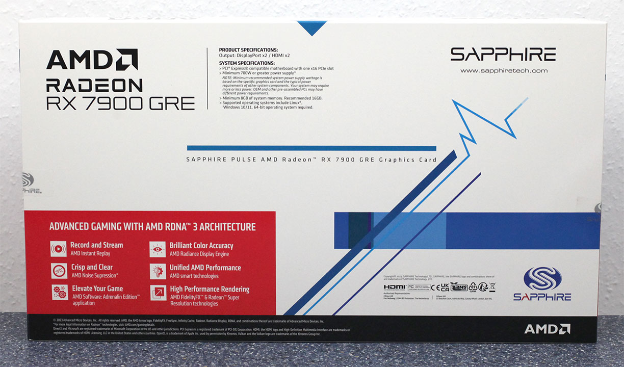
We have with us the Sapphire Radeon RX 7900 GRE Pulse, which we are treating as our de facto reference design review. There are made-by-AMD (MBA) reference design RX 7900 GRE cards out there, but those are restricted to the OEM channel, we neither could find them in retail, nor did AMD send us one. The Sapphire Pulse comes with a small factory overclock over the AMD baseline specs and features a well-balanced combination of a low-noise cooling solution, and a price that matches the $550 AMD MSRP.
Short 6-Minute Video Summarizing the RX 7900 GRE Pulse Review Results
Our goal with the videos is to create short summaries, not go into all the details and test results, which can be found in this written review.
| Price | Cores | ROPs | Core Clock | Boost Clock | Memory Clock | GPU | Transistors | Memory | |
|---|---|---|---|---|---|---|---|---|---|
| RTX 3070 | $310 | 5888 | 96 | 1500 MHz | 1725 MHz | 1750 MHz | GA104 | 17400M | 8 GB, GDDR6, 256-bit |
| RTX 3070 Ti | $350 | 6144 | 96 | 1575 MHz | 1770 MHz | 1188 MHz | GA104 | 17400M | 8 GB, GDDR6X, 256-bit |
| RX 6800 | $450 | 3840 | 96 | 1815 MHz | 2105 MHz | 2000 MHz | Navi 21 | 26800M | 16 GB, GDDR6, 256-bit |
| RX 7700 XT | $430 | 3456 | 96 | 2171 MHz | 2544 MHz | 2250 MHz | Navi 32 | 26500M | 12 GB, GDDR6, 192-bit |
| RX 6800 XT | $500 | 4608 | 128 | 2015 MHz | 2250 MHz | 2000 MHz | Navi 21 | 26800M | 16 GB, GDDR6, 256-bit |
| RTX 3080 | $450 | 8704 | 96 | 1440 MHz | 1710 MHz | 1188 MHz | GA102 | 28000M | 10 GB, GDDR6X, 320-bit |
| RTX 4070 | $525 | 5888 | 64 | 1920 MHz | 2475 MHz | 1313 MHz | AD104 | 35800M | 12 GB, GDDR6X, 192-bit |
| RX 7800 XT | $500 | 3840 | 96 | 2124 MHz | 2430 MHz | 2425 MHz | Navi 32 | 28100M | 16 GB, GDDR6, 256-bit |
| RX 6900 XT | $650 | 5120 | 128 | 2015 MHz | 2250 MHz | 2000 MHz | Navi 21 | 26800M | 16 GB, GDDR6, 256-bit |
| RX 6950 XT | $630 | 5120 | 128 | 2100 MHz | 2310 MHz | 2250 MHz | Navi 21 | 26800M | 16 GB, GDDR6, 256-bit |
| RTX 3090 | $800 | 10496 | 112 | 1395 MHz | 1695 MHz | 1219 MHz | GA102 | 28000M | 24 GB, GDDR6X, 384-bit |
| RTX 4070 Super | $590 | 7168 | 80 | 1980 MHz | 2475 MHz | 1313 MHz | AD104 | 35800M | 12 GB, GDDR6X, 192-bit |
| RX 7900 GRE | $550 | 5120 | 160 | 1880 MHz | 2245 MHz | 2250 MHz | Navi 31 | 57700M | 16 GB, GDDR6, 256-bit |
| Sapphire RX 7900 GRE Pulse | $550 | 5120 | 160 | 1927 MHz | 2293 MHz | 2250 MHz | Navi 31 | 57700M | 16 GB, GDDR6, 256-bit |
| RTX 4070 Ti | $720 | 7680 | 80 | 2310 MHz | 2610 MHz | 1313 MHz | AD104 | 35800M | 12 GB, GDDR6X, 192-bit |
| RTX 4070 Ti Super | $800 | 8448 | 96 | 2340 MHz | 2610 MHz | 1313 MHz | AD103 | 45900M | 16 GB, GDDR6X, 256-bit |
| RX 7900 XT | $700 | 5376 | 192 | 2000 MHz | 2400 MHz | 2500 MHz | Navi 31 | 57700M | 20 GB, GDDR6, 320-bit |
| RTX 3090 Ti | $1050 | 10752 | 112 | 1560 MHz | 1950 MHz | 1313 MHz | GA102 | 28000M | 24 GB, GDDR6X, 384-bit |
| RTX 4080 | $1200 | 9728 | 112 | 2205 MHz | 2505 MHz | 1400 MHz | AD103 | 45900M | 16 GB, GDDR6X, 256-bit |
| RTX 4080 Super | $1300 | 10240 | 112 | 2295 MHz | 2550 MHz | 1438 MHz | AD103 | 45900M | 16 GB, GDDR6X, 256-bit |
| RX 7900 XTX | $910 | 6144 | 192 | 2300 MHz | 2500 MHz | 2500 MHz | Navi 31 | 57700M | 24 GB, GDDR6, 384-bit |
| RTX 4090 | $1850 | 16384 | 176 | 2235 MHz | 2520 MHz | 1313 MHz | AD102 | 76300M | 24 GB, GDDR6X, 384-bit |
AMD RDNA 3 Graphics Architecture
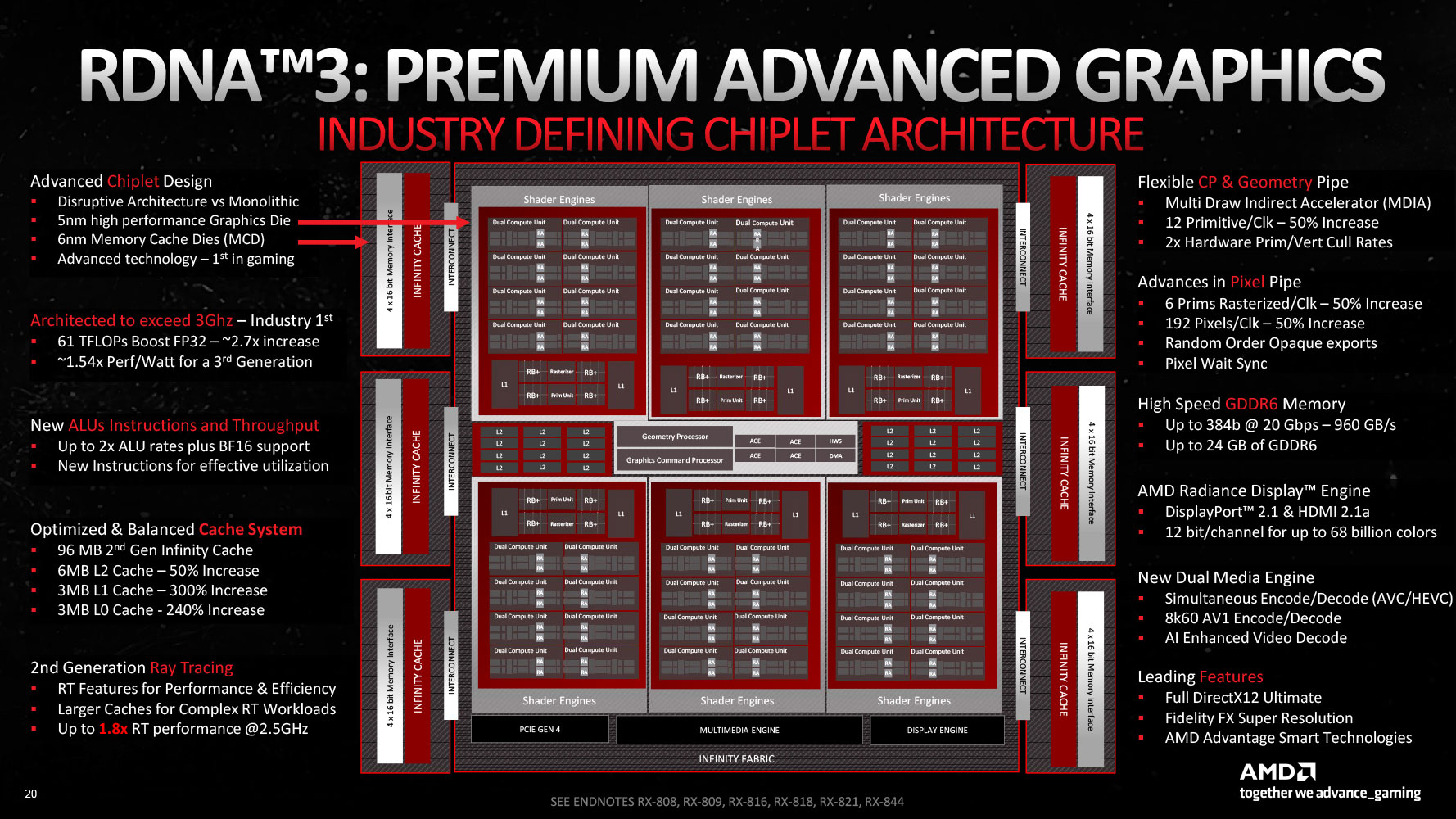
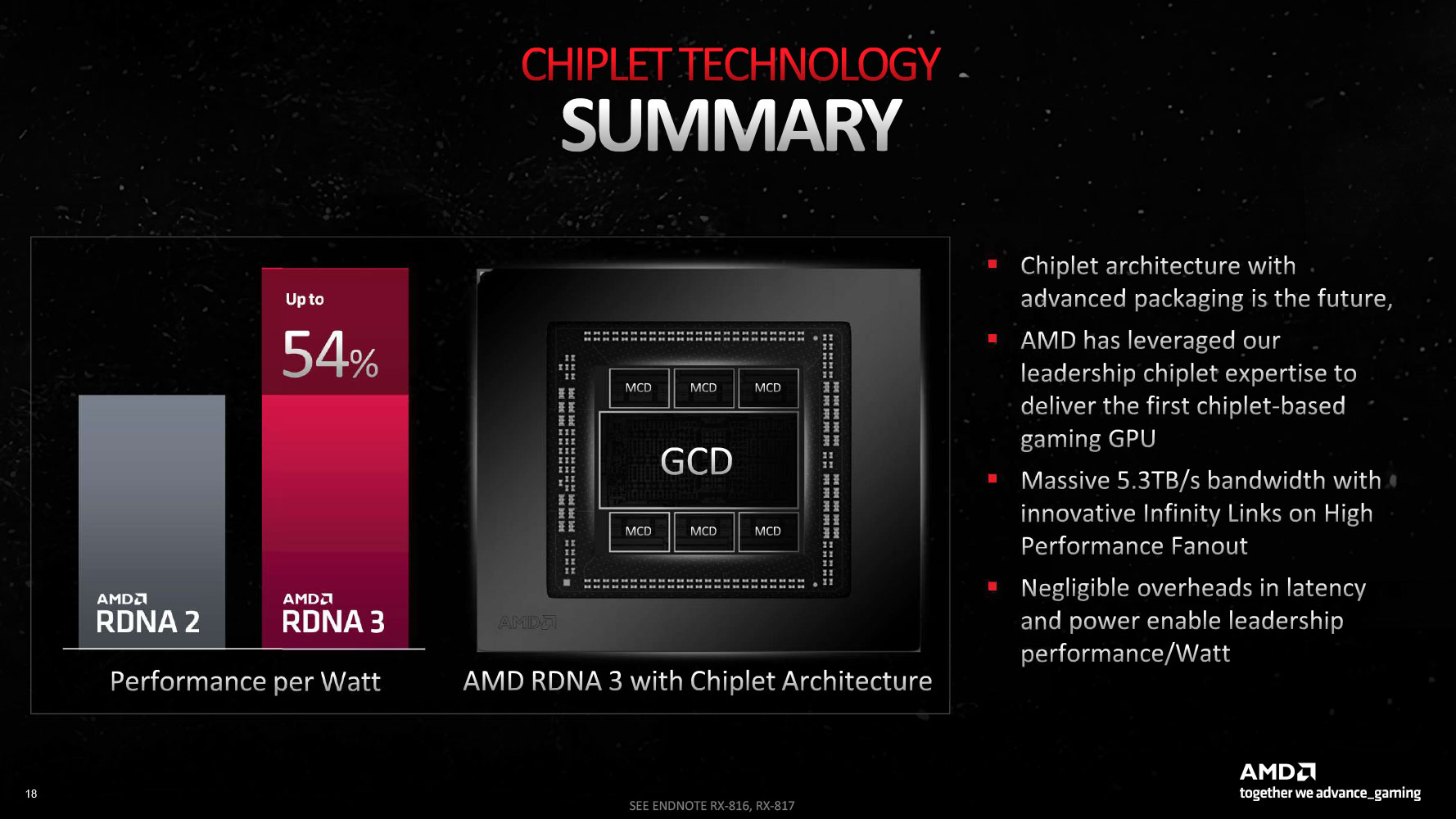
The Radeon RX 7900 series debuts AMD's 3rd generation RDNA graphics architecture, termed RDNA 3. With it, AMD plans to repeat the generational 50% performance/Watt gain it achieved with RDNA 2, which sprung it back to the high-end graphics segment after a long gap. AMD claims it succeeded in this endeavor, with a 54% generational performance/Watt gain. At the heart of this effort is the switch to the new TSMC 5 nm EUV foundry node. AMD figured out early on that it cannot build large monolithic GPUs on 5 nm without thinning its margins in the fight against NVIDIA, and set out to innovate the Chiplet architecture for the GPU. Under this, specific parts of the GPU that actually benefit from a switch to a newer foundry node, such as the Shader Engines, would be built on a centralized 5 nm die called the Graphics Compute Die (GCD), while those components that can make do with a less advanced node, namely the memory controllers and L3 cache, would be spun off to chiplets called Memory Cache Dies (MCDs), built on 6 nm.

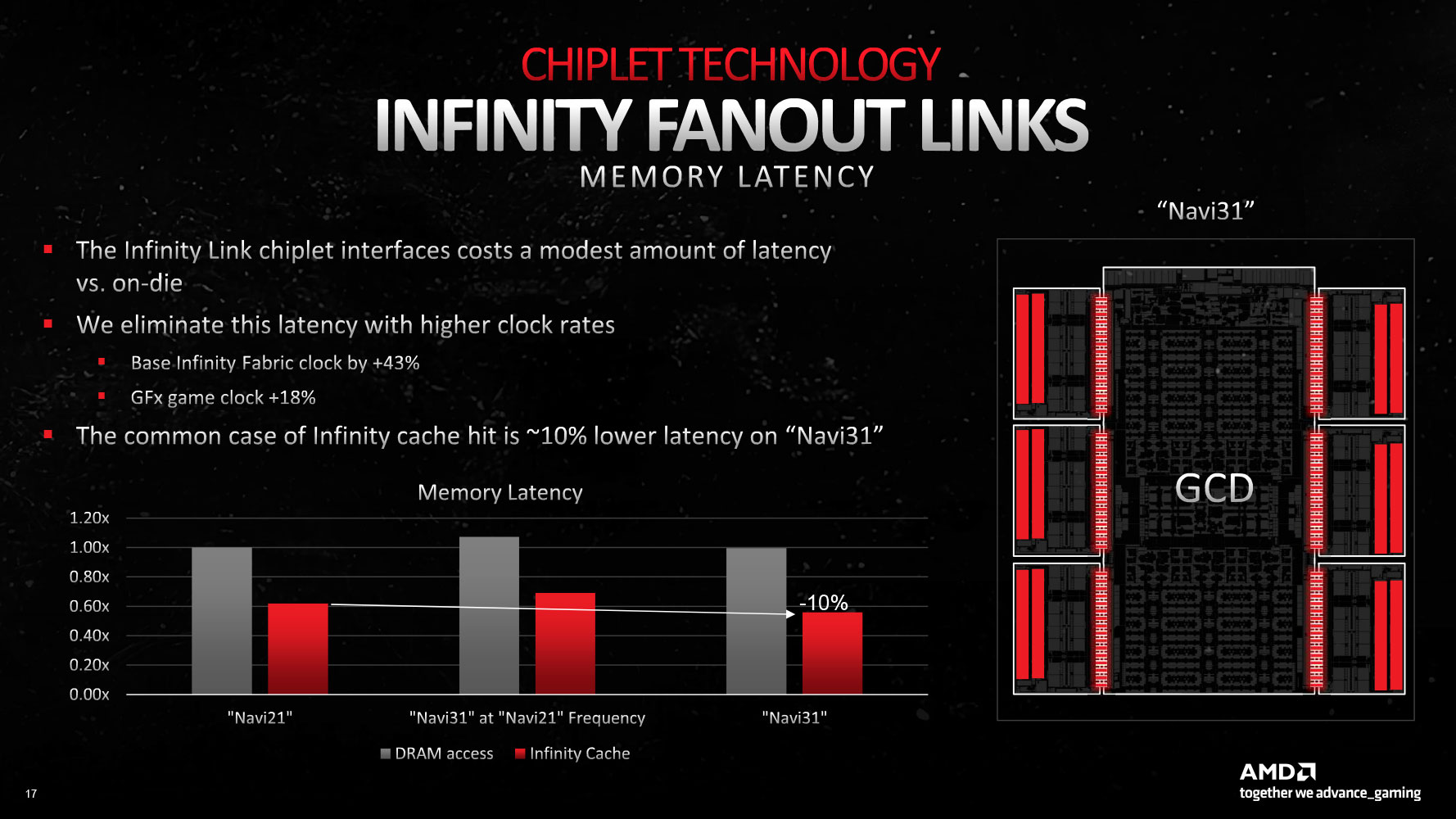
The "Navi 31" GPU is hence a chiplet GPU and not a multi-chip module like "Vega 10." In a chiplet-based device, various components that can otherwise not exist on their own packages, are placed on a single package, with the goal of minimizing production costs, by stratifying their need for a new foundry node, such that only the most power-intensive IP receive the most advanced node. In a MCM, chips that can otherwise exist on their own package, are combined onto a single package for conserving PCB real-estate, or reducing latency. The GCD in the "Navi 31" GPU hence has all the shader engines, caches up to L2, the front-end Command Processor, Async Compute Engines (ACEs), the Display Engine, and the Media Engine. Each of the six MCDs has a 64-bit wide memory bus, and a 16 MB segment of the GPU's 96 MB Infinity Cache memory. The size of the Infinity Cache may have been generationally reduced (compared to 128 MB on "Navi 21"), but AMD has widened the memory bus itself, from 256-bit up to 384-bit.
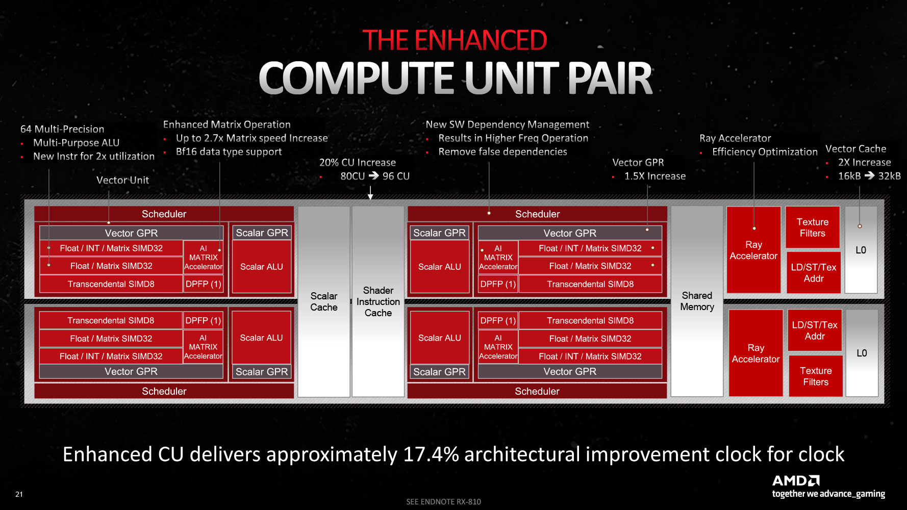
Much of the architectural innovation is not with the chiplet design (a packaging innovation); but at the level of the RDNA 3 Dual-Compute Unit (or Compute Unit pair). The "Navi 31" GPU physically features 96 compute units spread across six Shader Engines. AMD claims that at the same engine clocks, the RDNA 3 CU offers a 17.4% IPC increase over the RDNA 2 CU. There are 20% more CUs over the "Navi 21," and these run at higher engine clocks, tapping into the power headroom afforded by the 5 nm process. These combined work out to the 54% generational performance uplift, with which AMD plans to retain competitiveness with NVIDIA's RTX 40-series "Ada" high-end SKUs.
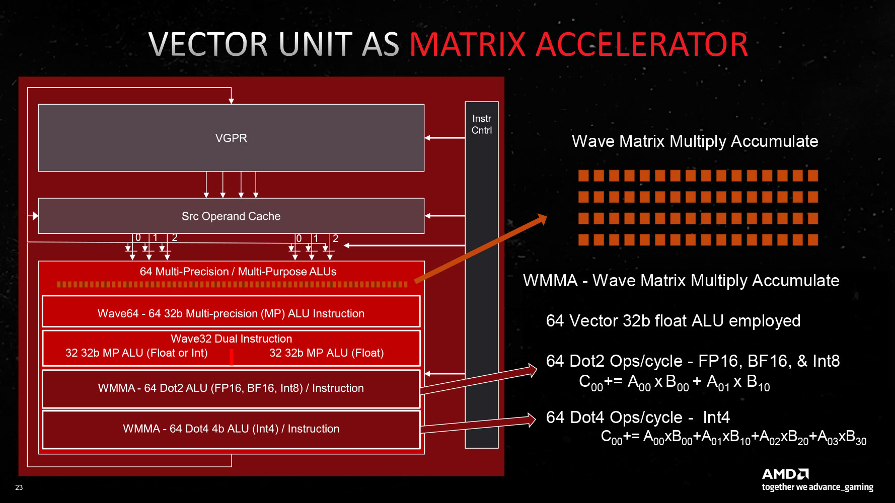
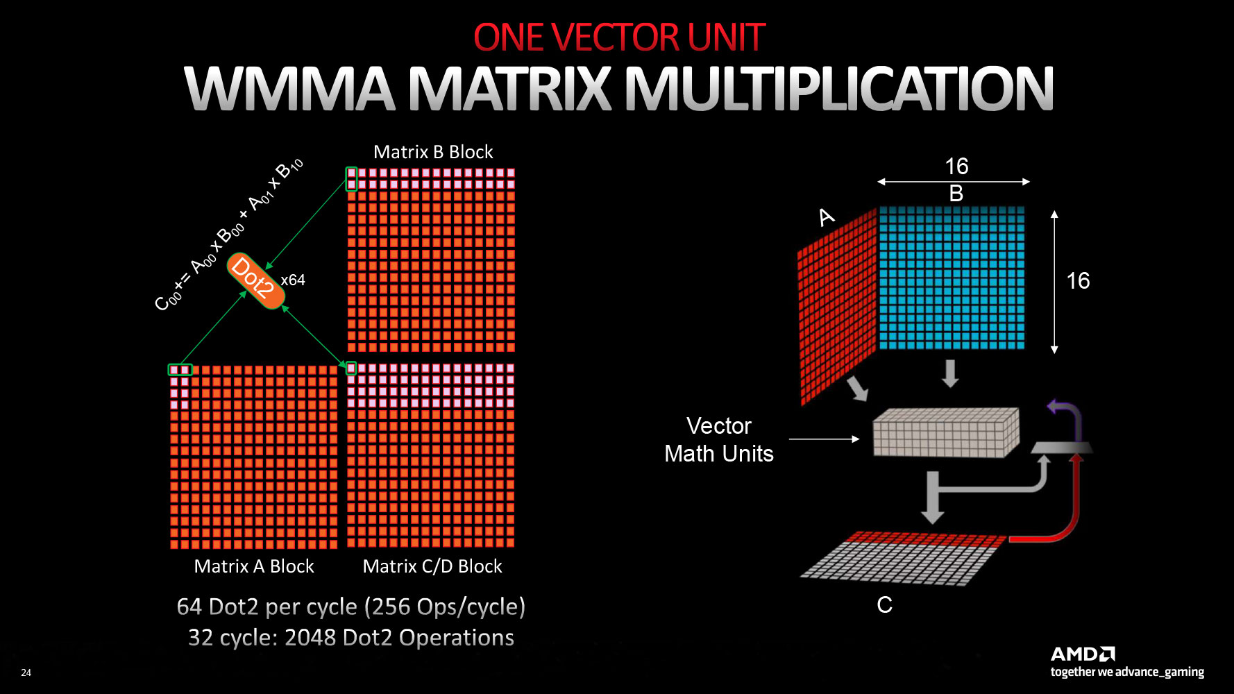
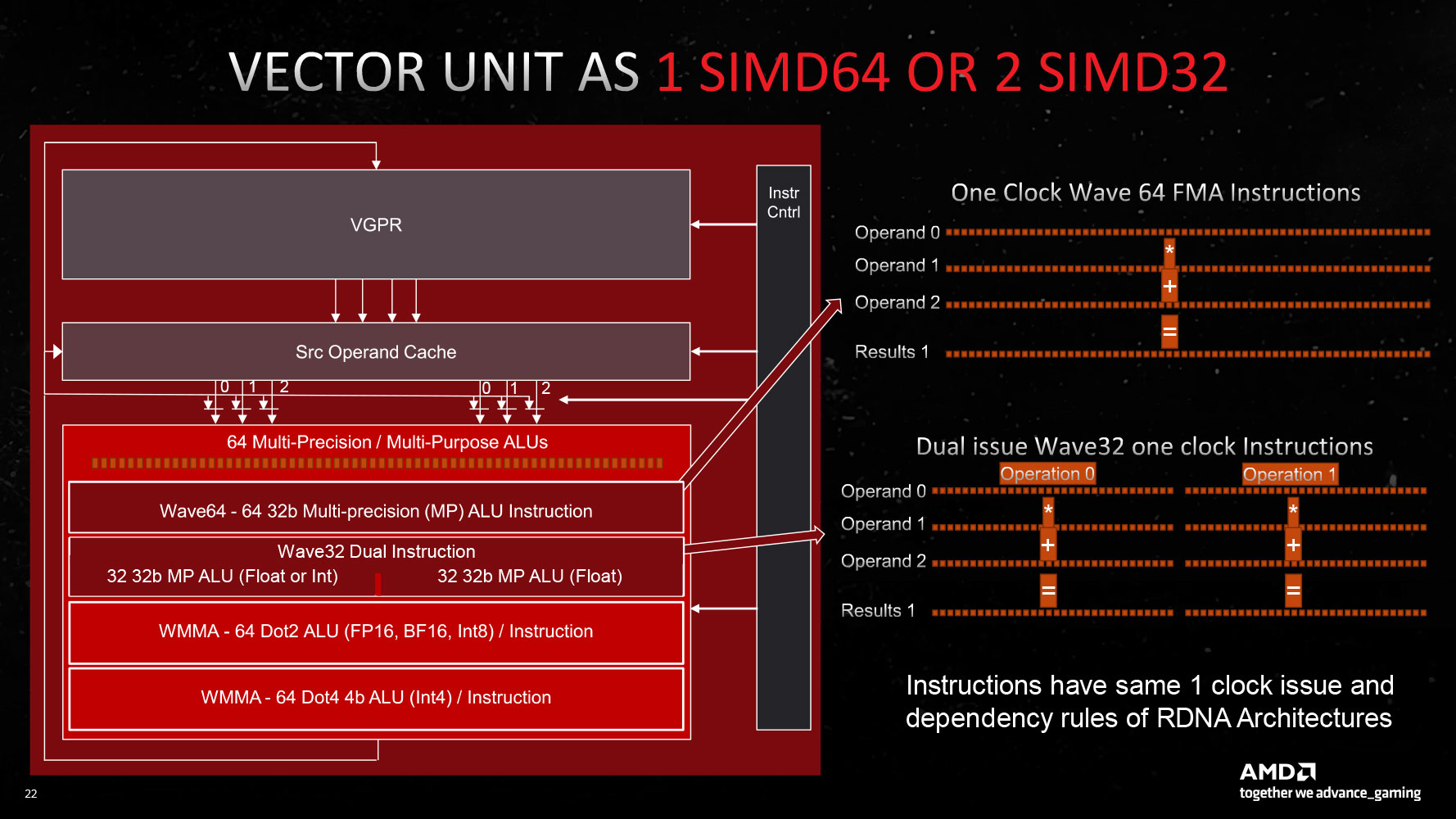
The new RDNA 3 CU introduces multi-precision capability for the 64 stream processors per CU: operating either as 1x SIMD64 or 2x SIMD32 units. The Vector Unit that houses these SIMD units can either function as a SIMD execution mechanism, or as a Matrix execution unit, thanks to the new AI Matrix Accelerator, which provides a 2.7x matrix multiplication performance uplift versus conventional SIMD execution. Also added are support for the Bfloat16 instruction-set, and SIMD8 execution. The GPU hence enjoys AI hardware-acceleration that can be leveraged in future feature-additions relevant to gamers, such as FSR 3.0. Game developers will also look for ways to exploit accelerated AI, now that all three brands feature it (NVIDIA Tensor cores and Intel XMX cores).
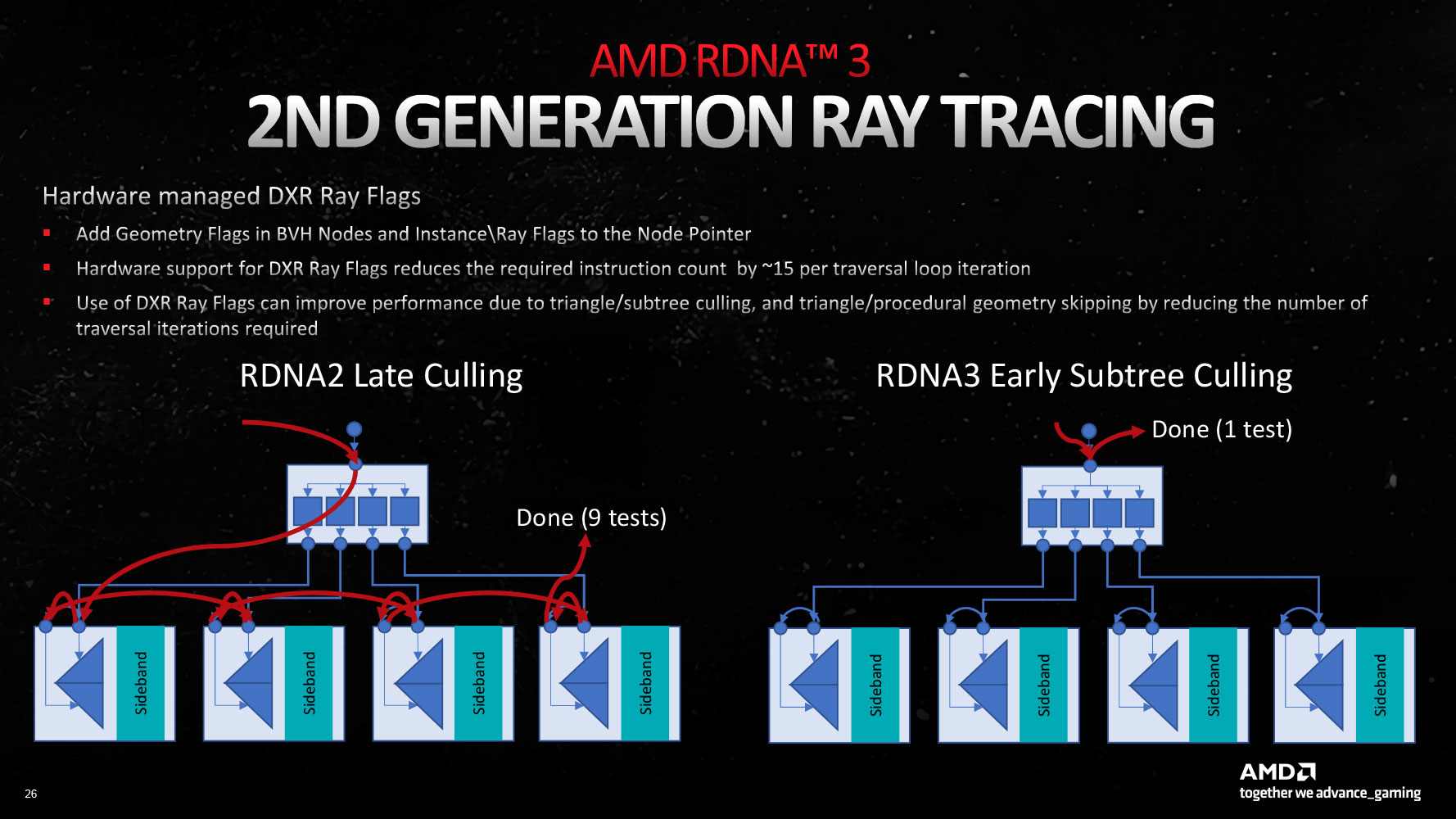
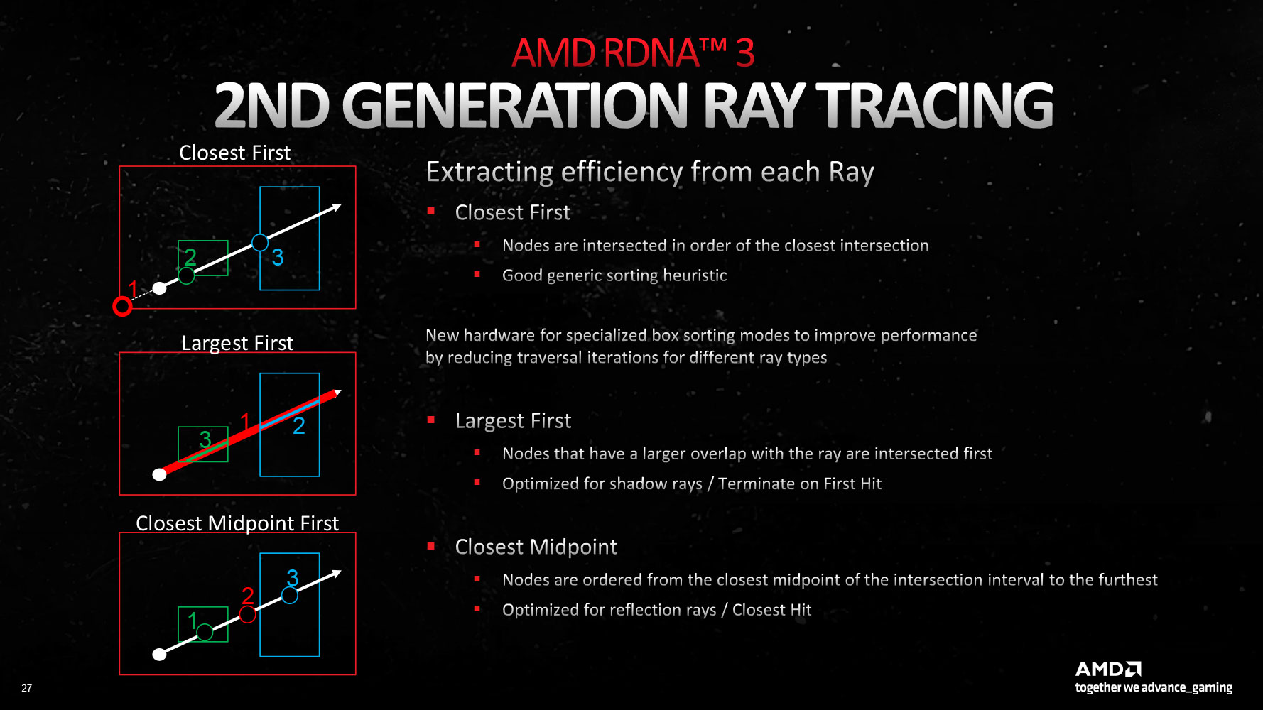
AMD's first-generation Ray Accelerator, introduced with the RDNA 2 architecture, was the result of a hasty effort to catch up to NVIDIA with a DirectX 12 Ultimate GPU, where they developed a fixed-function hardware to calculate ray intersections, and offloaded a large chunk of RT processing to the generationally-doubled SIMD resources. With RDNA 3, they've refined the Ray Accelerator to achieve an 80% ray tracing performance uplift over the previous generation, when you add up the Ray Accelerator count, their higher engine clocks, and other hardware-level optimizations, such as early subtree culling, specialized box sorting modes, and reduced traversal iterations.

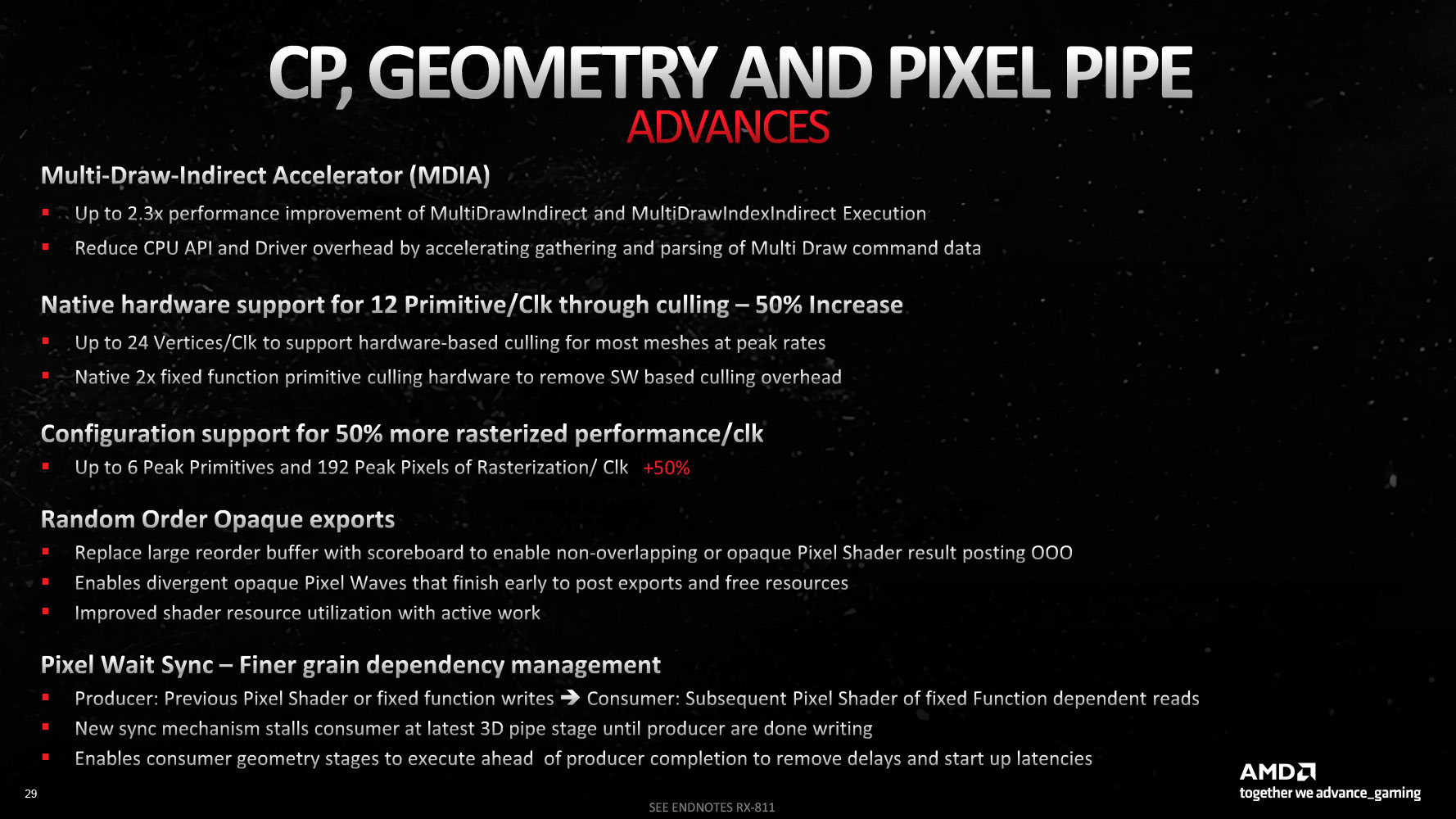
There is a 50% ray intersection capacity improvement for the "Navi 31" GPU thanks to these optimizations, and cycles-per-ray reduction. Besides these, AMD has also made several improvements to the geometry- and pixel-pipes, with the introduction of the new multi-draw indirect accelerator (MDIA), which reduces CPU API and driver-level overheads by gathering and parsing of multi-draw command data. At the hardware-level 12 primitives per clock is now supported compared to 8 per clock on RDNA 2, thanks to culling. The core-configuration overall enables 50% more rasterized performance per clock.
The GCD features six Shader Engines, each with 16 compute units (or 8 dual compute units), which work out to 1,024 stream processors. Six such Shader Engines make up 6,144 stream processors with 96 Ray Accelerators and 96 AI Accelerators. The GPU has 384 TMUs, and a massive 192 ROPs—a 50% increase over "Navi 21." The Radeon RX 7900 XTX enables all 96 CUs, and maxes out the silicon, whereas the RX 7900 XT has 84 out of 96 CUs enabled, which work out to 5,376 stream processors, 84 Ray Accelerators, 336 TMUs, and an unchanged 192 ROPs. The new RX 7900 GRE has 80 CUs enabled, which work out to 5,120 stream processors, 80 Ray Accelerators, 320 TMUs, and 160 ROPs. The RX 7900 XTX gets 24 GB of GDDR6 memory across the GPU's entire 384-bit memory bus, with a memory speed of 20 Gbps (GDDR6-effective), which means 960 GB/s of memory bandwidth. The RX 7900 XT is equipped with 20 GB of memory across a narrower 320-bit memory bus carved out by disabling one of the six MCDs. At the same 20 Gbps speed, this yields 800 GB/s bandwidth. The RX 7900 GRE goes one further step down, with two of the six MCDs being disabled, for a 256-bit memory bus, running 16 GB of memory at 18 Gbps speed, for 576 GB/s of bandwidth.
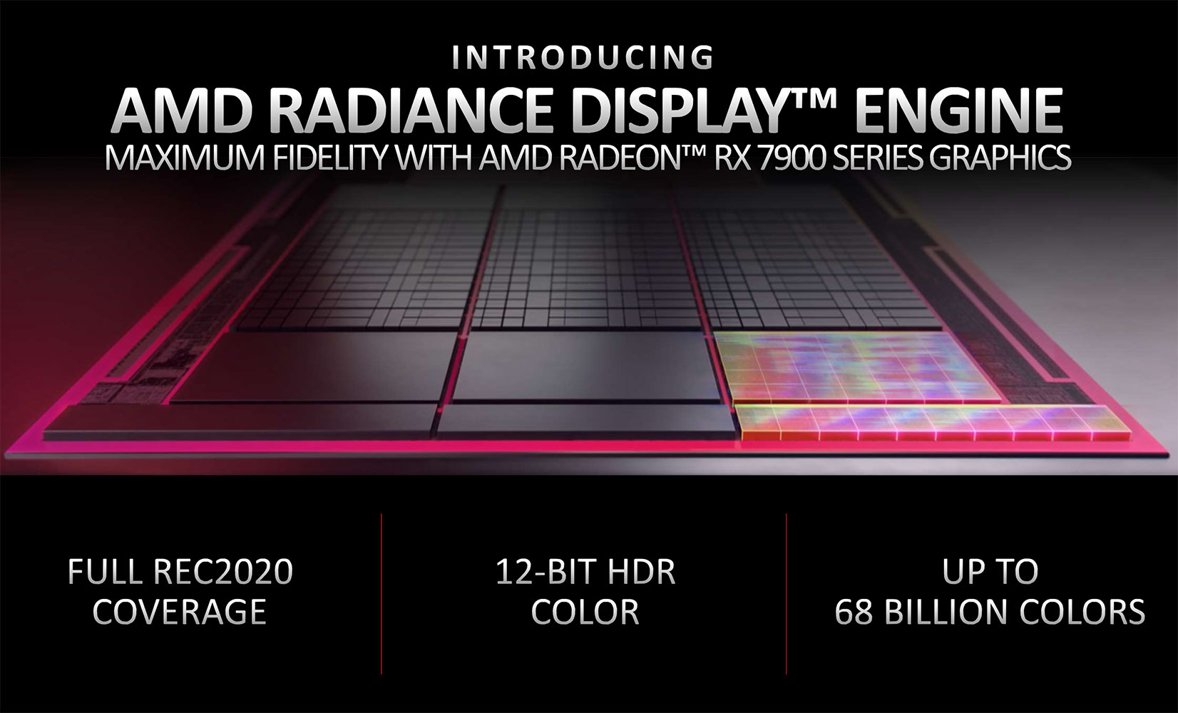
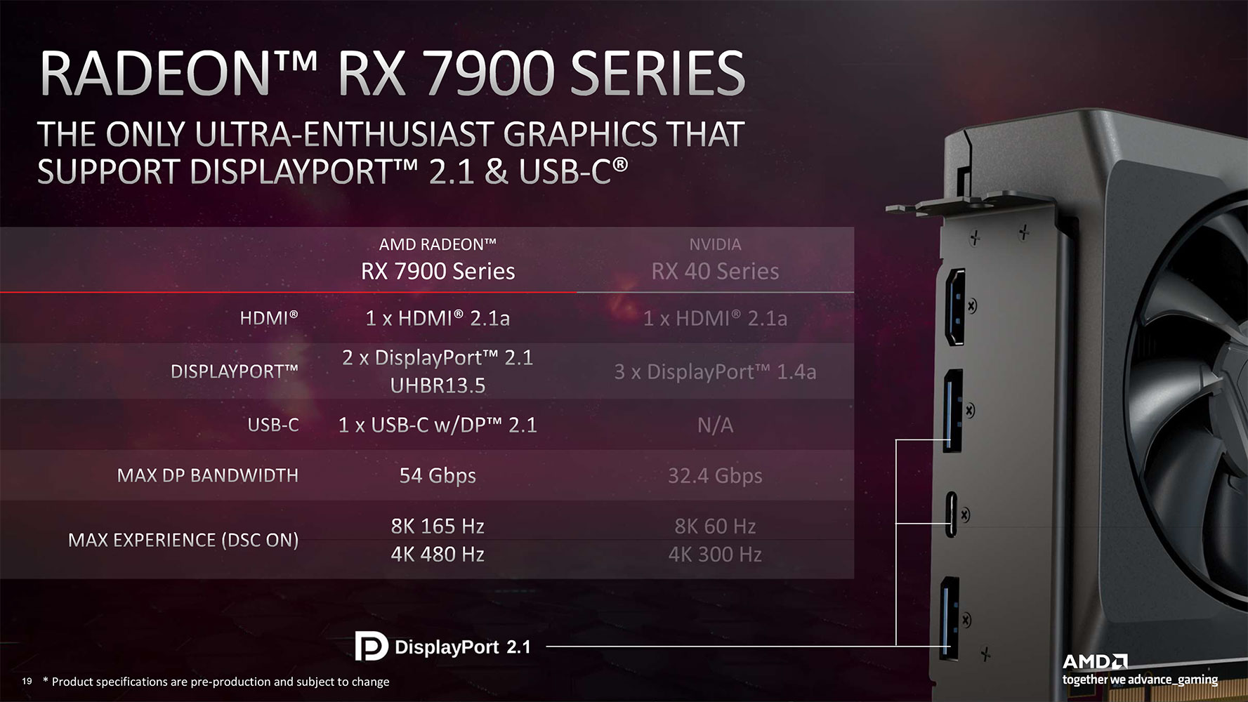
AMD has significantly improved the Display Engine of "Navi 31" over the previous-generation in terms of connectivity. The new Radiance Display Engine comes with native support for DisplayPort 2.1, which enables 8K output at up to 165 Hz refresh-rate, or 4K at up to 480 Hz, with a single cable. AMD has refined its FSR 2 algorithm to support 8K (i.e. render at a lower resolution with FSR-enhanced upscaling), to make it possible to enjoy the latest AAA titles at playable frame-rates on 8K displays. Both the RX 7900 series cards get two full-size DP 2.1 connectors, besides an HDMI 2.1b, and a USB-C with DP 1.2 passthrough. The "Navi 31" silicon receives full hardware-accelerated AV1 encode and decode capabilities, through dual independent encode/decoders, so two independent video streams can be simultaneously transcoded, or one stream at twice the framerate. With this generation, AMD is also introducing SmartAccess Video, a feature that lets the AMD driver leverage the hardware encoders of the RDNA 2 iGPU of Ryzen 7000 desktop processors, for additional encoding performance.
FidelityFX SuperResolution 3 Fluid Motion Frames (FSR 3 and FMF)
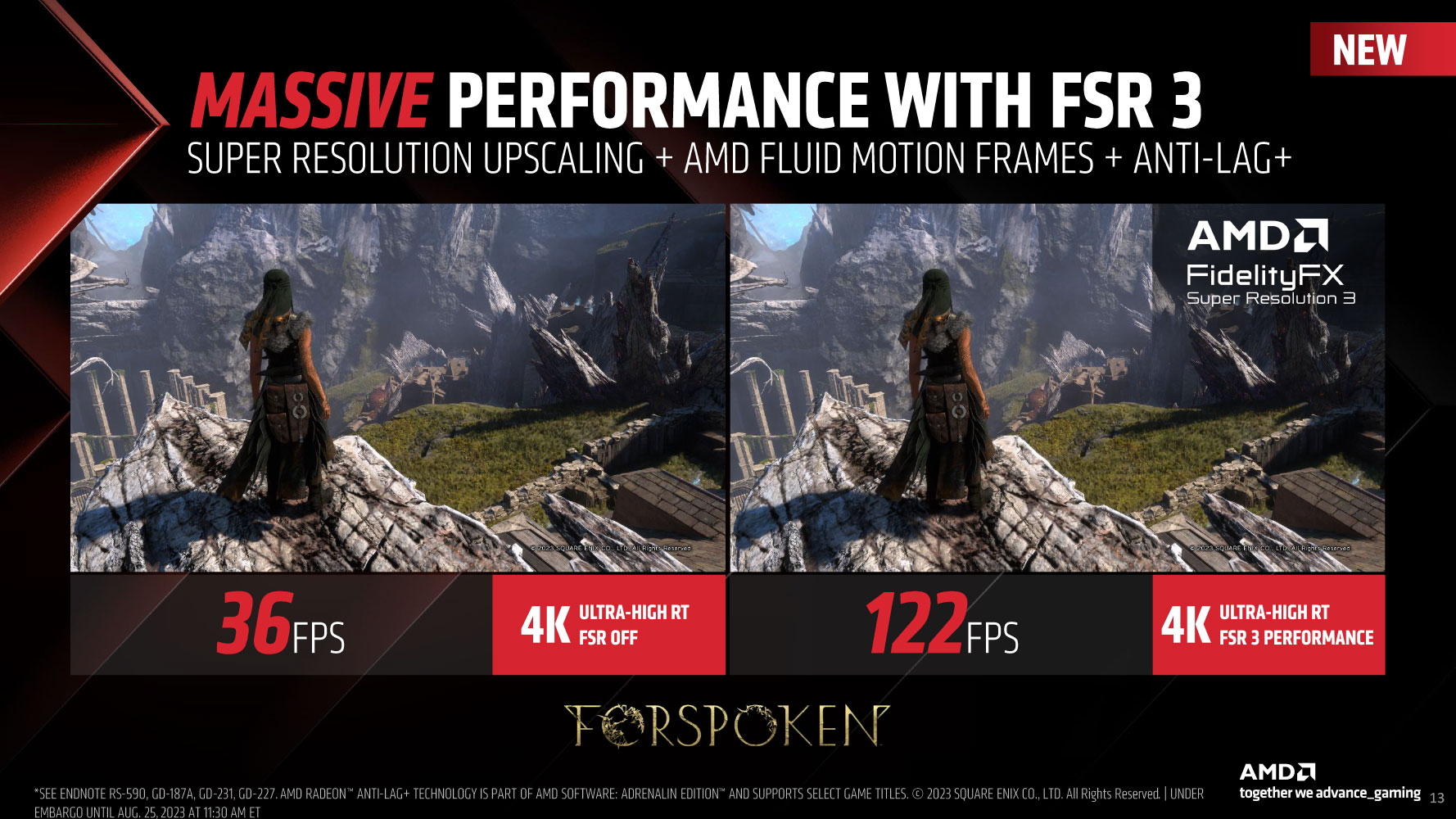
AMD announced the much awaited FidelityFX Super Resolution 3 and Fluid Motion Frames. FSR 3 is being announced as a technological rival to NVIDIA DLSS 3 Frame Generation. The premise with both technologies is the same—to effectively double frame-rates by generating alternate frames without running them through the entire graphics rendering pipeline, it's just that the two technologies differ in their approach to this goal.
FSR 3 builds on FSR 2 with its updated super resolution upscaler promising generational quality improvements at a every given rendering resolution. Fluid Motion Frames (FMF) isn't the entirety of the FSR 3 feature-set, but is its most important feature-addition. FMF is a frame interpolation technology much like the one consumer televisions come with. Alternate frames are generated as an approximate of two frames. Where FMF differs from DLSS 3 Frame Generation is that while NVIDIA uses a hardware component called optical flow accelerator and the GPU's AI acceleration to generate an intermediate frame without involving the graphics rendering pipeline, FMF uses a certain amount of the graphics rendering pipeline. At a hardware level, FMF uses the main SIMD machinery of the GPU, leveraging asynchronous compute. As with DLSS 3 FG, FSR 3 FMF comes with added latency. NVIDIA counteracts this with Reflex, while AMD uses Radeon AntiLag+. Both technologies try to keep the frame queue short to reduce whole system latencies.
One major advantage FSR 3 FMF enjoys over DLSS 3 FG is that it works on any modern DirectX 12 GPU that supports async compute, since it doesn't require a specific hardware component the way DLSS 3 FG requires the Optical Flow Accelerator on NVIDIA "Ada" GPUs. The only limiting factor here is the performance. To be more specific, AMD says that all Radeon GPUs from RX 5700 series onward; and all GeForce GPUs from RTX 20-series onward, should support FSR 3 FMF. Also, FSR 3 FMF is as easy to integrate with games as FSR 2 is. The first games implementing FSR 3 FMF should arrive in Fall 2023. AMD is also working to extend FMF to Radeon Super Resolution, the driver-level technology that enables performance upscaling to even games that don't support FSR.
HYPR-RX
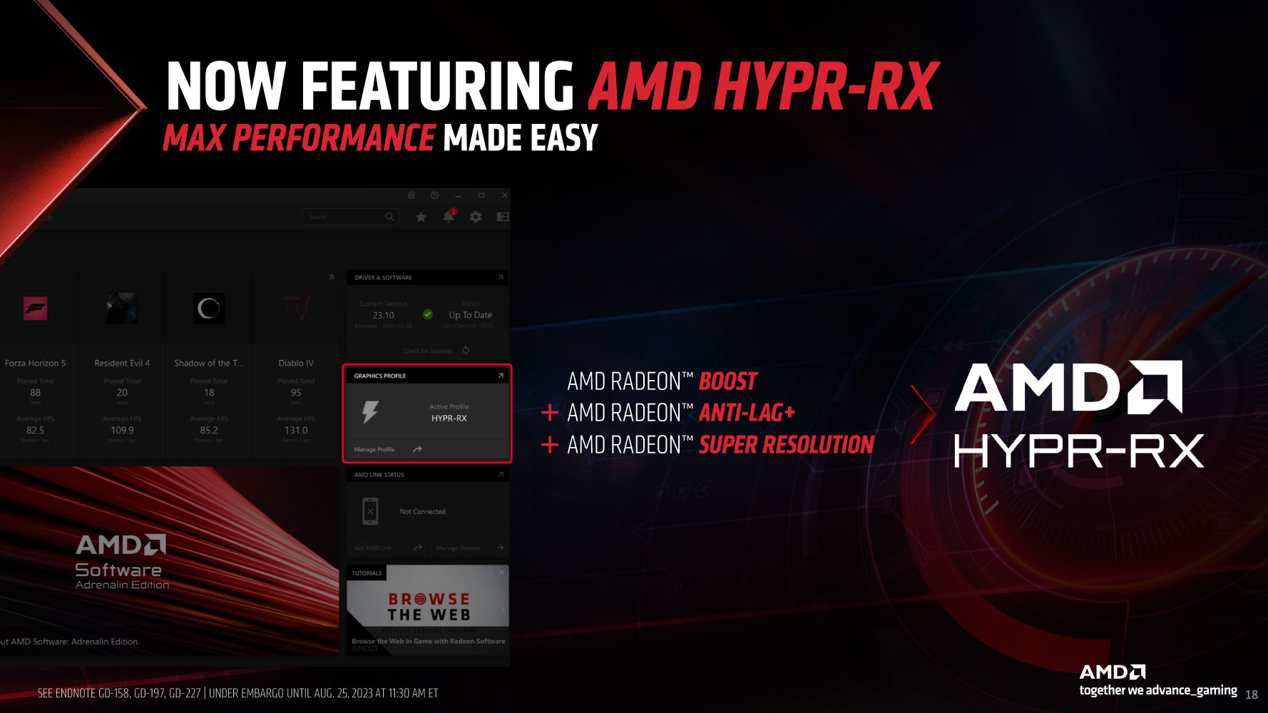
HYPR-RX is an interesting new feature in the AMD Software (control center) application. It is a one-click performance boosting technology that works with any DirectX 11 or DirectX 12 game. The software is a cocktail of Radeon Boost, Radeon AntiLag+, and Radeon Super Resolution, and applies the three features on any running game as needed, automatically. Radeon Boost improves performance by dynamically reducing the render resolution of a game when there's too much motion on the screen (and hence not enough detail needed). Radeon Super Resolution improves frame-rates as it applies FSR on the output of a game rendered at a lower resolution (including the frames lowered in resolution by Radeon Boost. AntiLag+ counteracts the latency added by these two, by shortening the frame queue. AFMF is part of the HYPR-RX feature-set, which can be activated with a single click.
Packaging
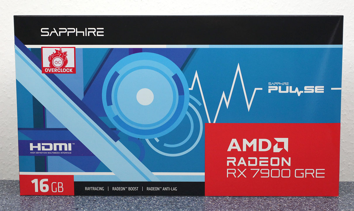
The Card
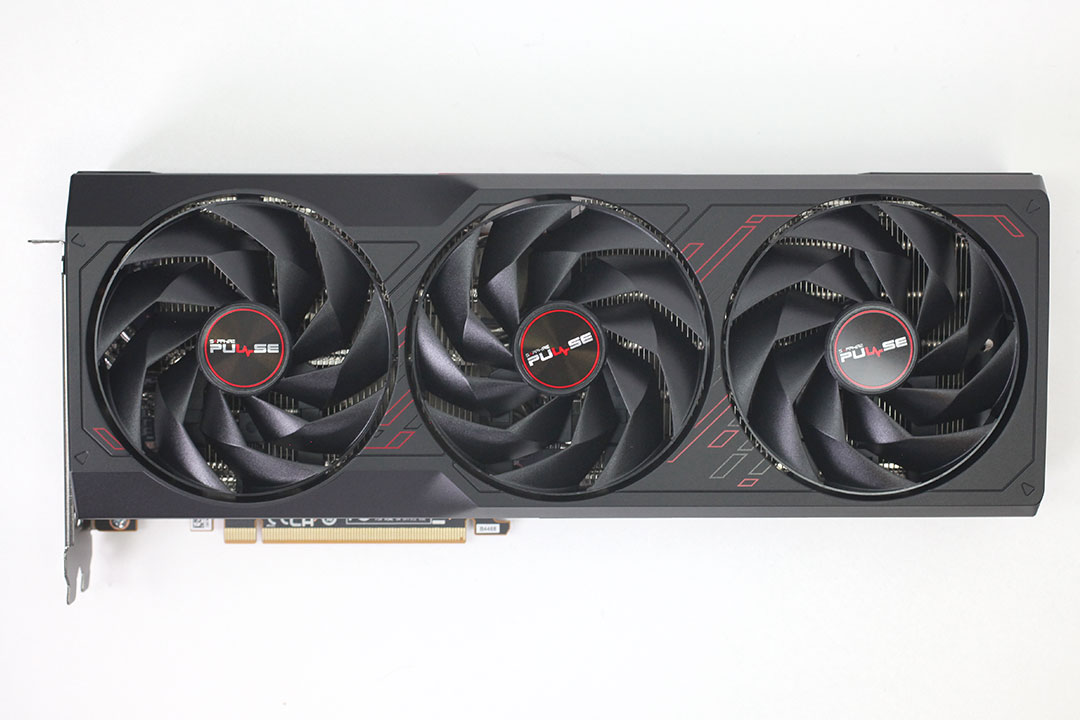
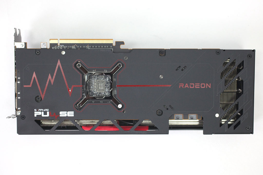
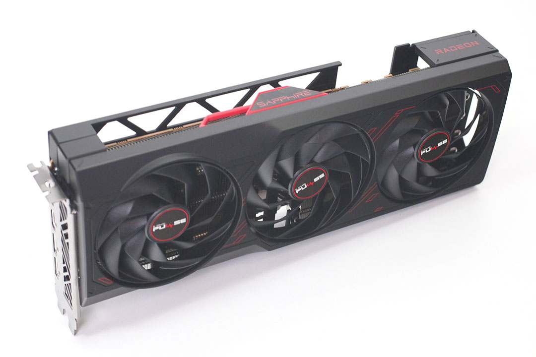
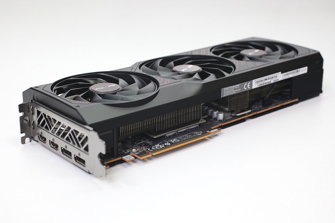
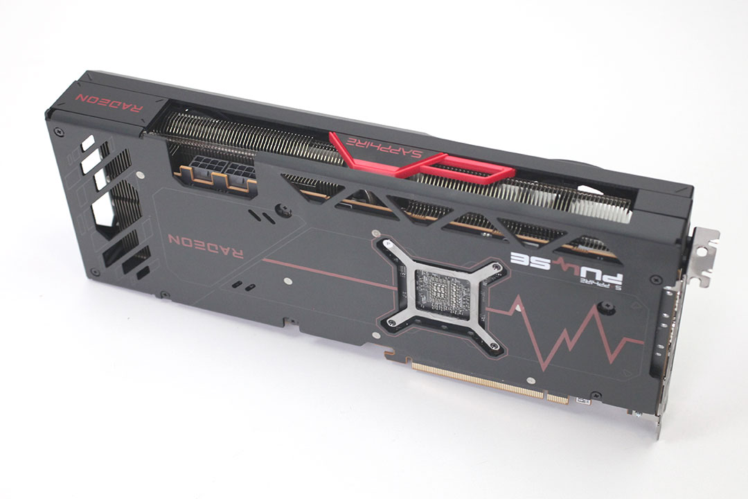
Sapphire Pulse design for the RX 7900 GRE follows the company's design theme for the Radeon RX 7900 Pulse, but there are subtle differences in both cooler and shroud, when compared to the RX 7900 XT Pulse. On the back you'll find a metal backplate, which is designed to let some airflow through the cooler.
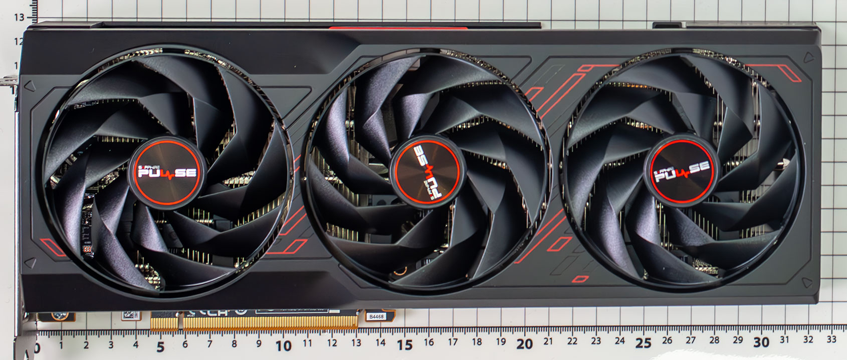
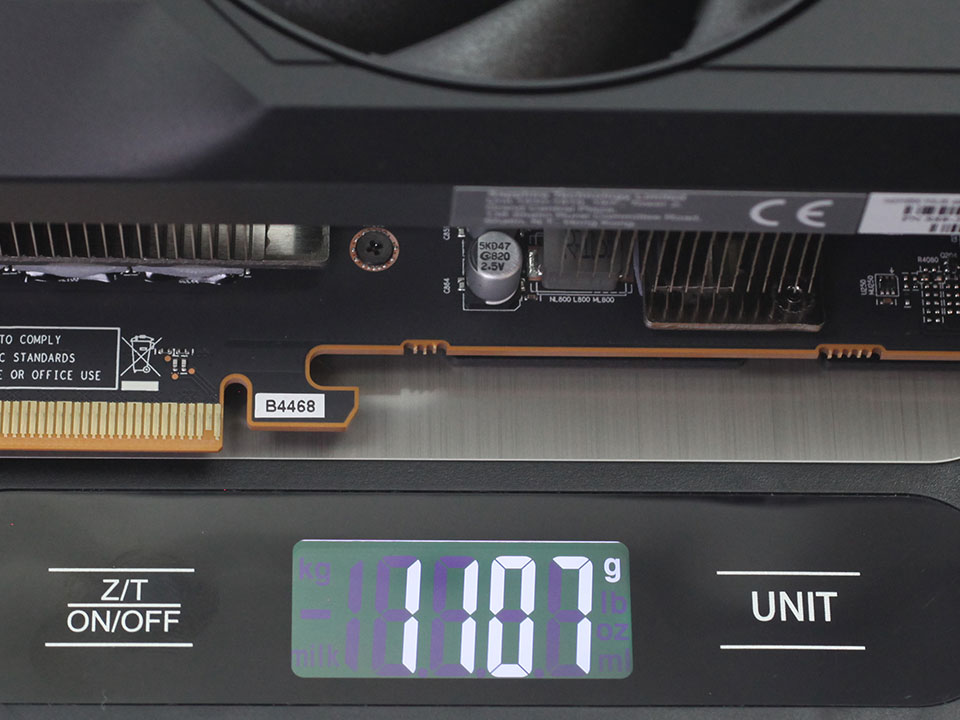
Dimensions of the card are 32.0 x 13.0 cm, and it weighs 1107 g.
Installation requires three slots in your system.
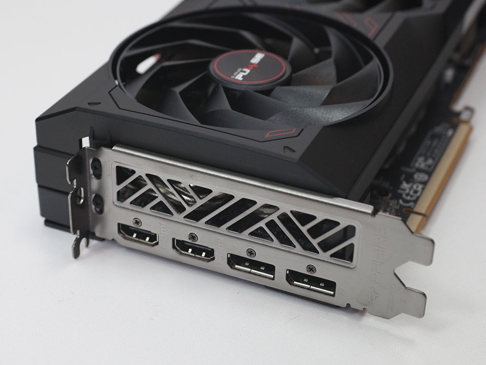
Display connectivity includes two standard DisplayPort 2.1 ports (RDNA 2 had 1.4a) and two HDMI 2.1a (same as RDNA 2).
AMD has upgraded their encode/decode setup. It now comes with two independent hardware units that can encode and decode two streams of video in parallel, or one stream at double the FPS rate. There's support for VP9, H.264, H.265 and AV1 decode, and encoding is supported for H.264, H.265 and AV1.
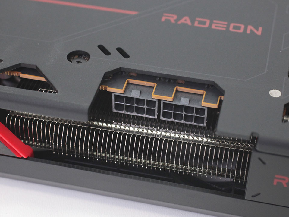
The card uses a classic dual 8-pin plus PCIe slot power input config, altogether rated for 375 W maximum power. NVIDIA on the other hand uses the new 12+4 pin ATX 12V-2x6 connector, which is rated for up to 600 W of power draw.
Our Patreon Silver Supporters can read articles in single-page format.
Aug 2nd, 2025 03:34 CDT
change timezone
Latest GPU Drivers
New Forum Posts
- Windows 12 (245)
- My UPS keep sending alarm when I game (39)
- What are you playing? (24030)
- What's your latest tech purchase? (24429)
- Free Games Thread (4838)
- 3DMARK "LEGENDARY" (359)
- memory used for store firmware in adapters wifi usb (4)
- Samsung 870 EVO - Beware, certain batches prone to failure! (1306)
- What antivirus do you use? (61)
- Laptop WWAN SSD? (4)
Popular Reviews
- ASUS ROG Crosshair X870E Apex Review
- MSI Claw 8 AI+ A2VM Review
- Montech X5 Review
- Orbital Pathfinder Review
- Herman Miller Logitech G Embody Review - No Pain, No Gain
- Lenovo Legion 5i (15IRX10) Review - Feature-Rich and Wallet Friendly
- Lian Li HydroShift II LCD-C 360TL Review
- Upcoming Hardware Launches 2025 (Updated May 2025)
- Noctua NF-A12x25 G2 PWM Fan Review
- Lian Li O11 Dynamic Mini V2 Review
TPU on YouTube
Controversial News Posts
- AMD's Upcoming UDNA / RDNA 5 GPU Could Feature 96 CUs and 384-bit Memory Bus (138)
- AMD Radeon RX 9070 XT Gains 9% Performance at 1440p with Latest Driver, Beats RTX 5070 Ti (131)
- Intel "Nova Lake-S" Core Ultra 3, Ultra 5, Ultra 7, and Ultra 9 Core Configurations Surface (110)
- DDR6 Memory Arrives in 2027 with 8,800-17,600 MT/s Speeds (102)
- NVIDIA to Debut GeForce RTX 50-series SUPER GPUs by Christmas (101)
- AMD Sampling Next-Gen Ryzen Desktop "Medusa Ridge," Sees Incremental IPC Upgrade, New cIOD (97)
- Intel CEO Confirms SMT To Return to Future CPUs (95)
- NVIDIA Becomes First Company Ever to Hit $4 Trillion Market-Cap (94)