 32
Sapphire Radeon RX 9060 XT Pulse OC 16 GB Review - An Excellent Choice
Test Setup »High-resolution PCB Pictures
These pictures are for the convenience of volt modders and people who would like to see all the finer details on the PCB. Feel free to link back to us and use these in your articles, videos or forum posts.

High-resolution versions are also available (front, back).
Circuit Board (PCB) Analysis


A 7-phase VRM powers the GPU. It is managed by a Monolithic Power Systems MP2868A controller.
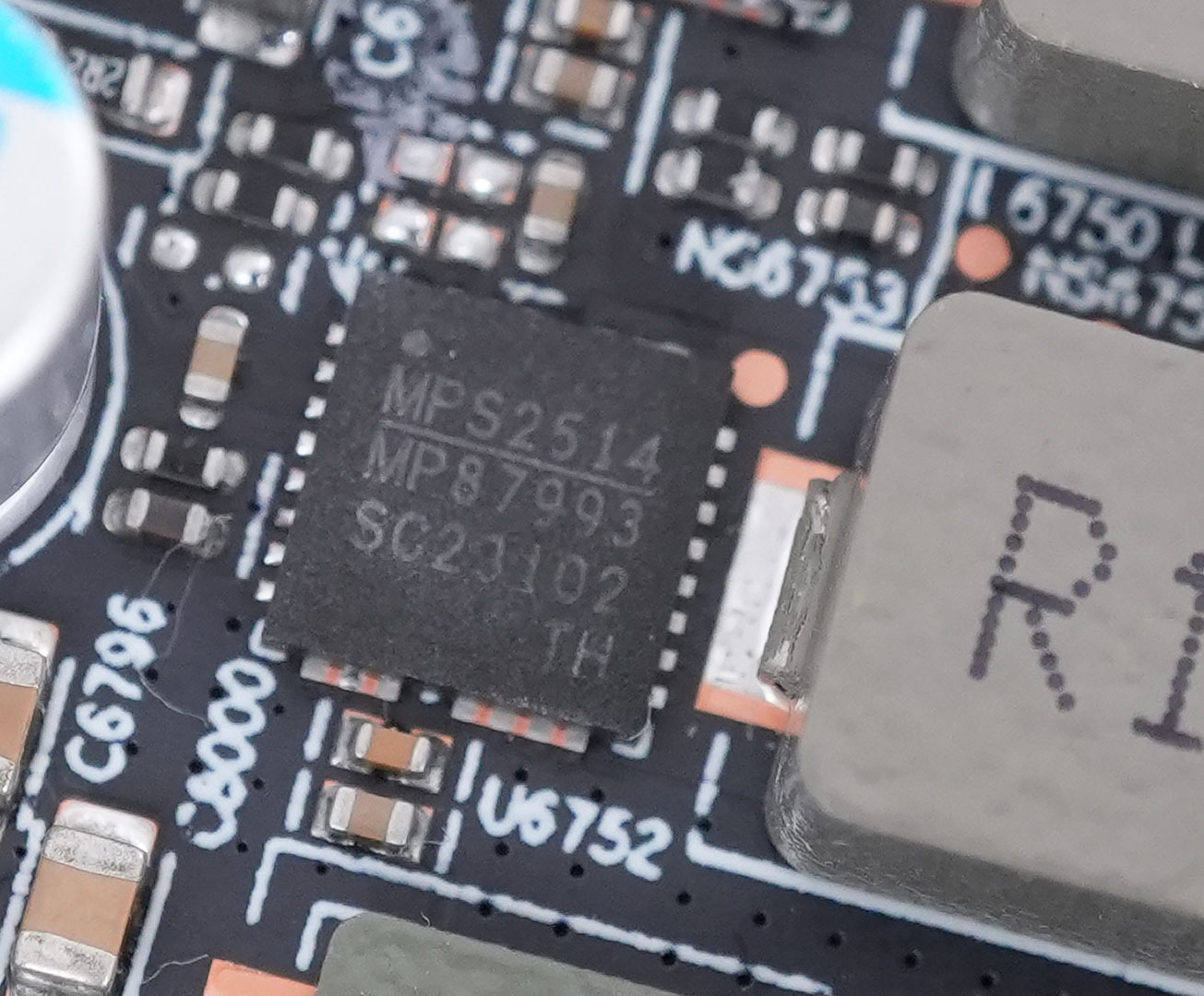
All GPU power phases use Monolithic MPS MP87993 DrMOS with a rating of 50 A.

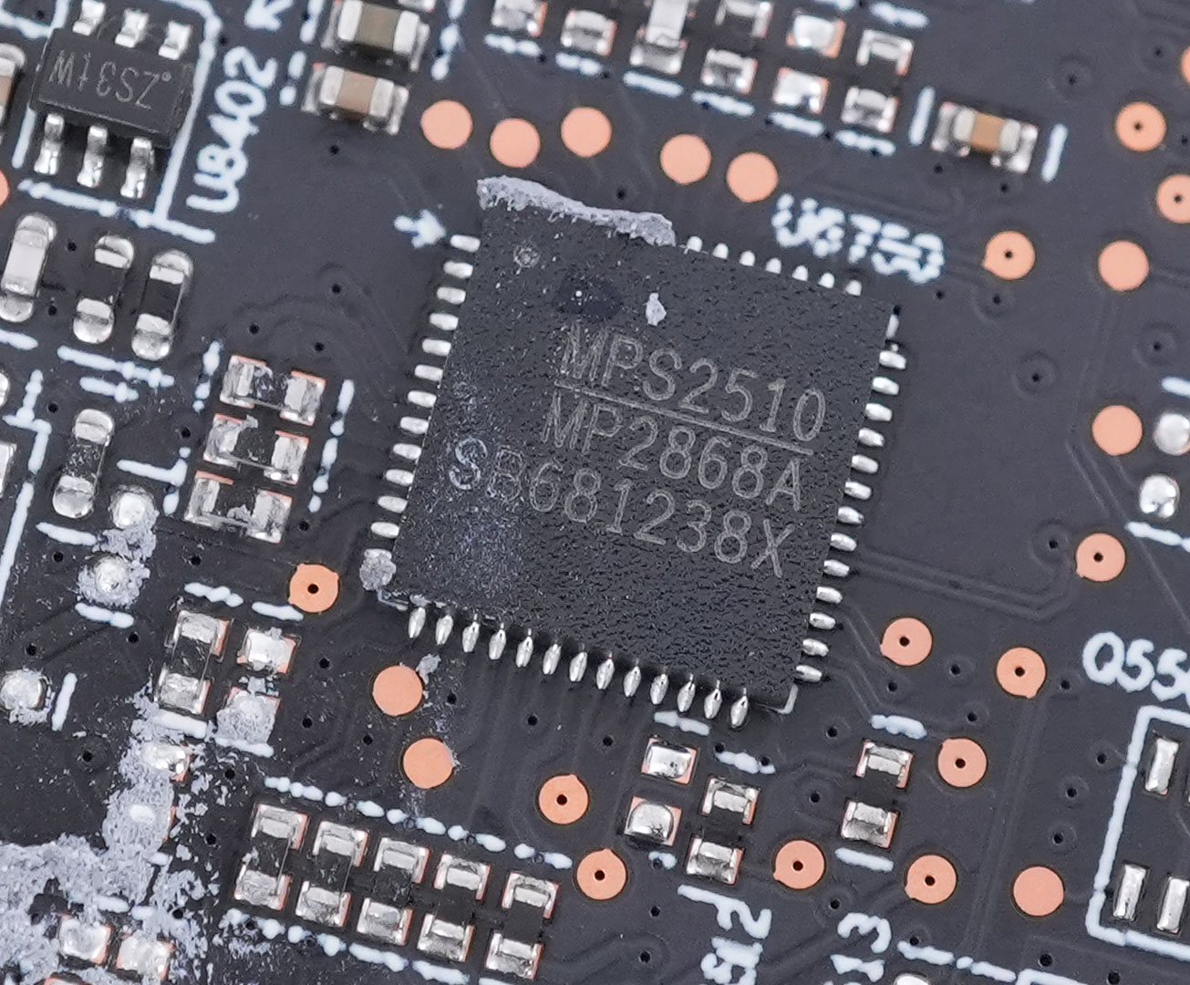
Powering the GDDR6 memory chips is a 1+1 phase VRM driven by a second Monolithic Power Systems MP2868A controller.
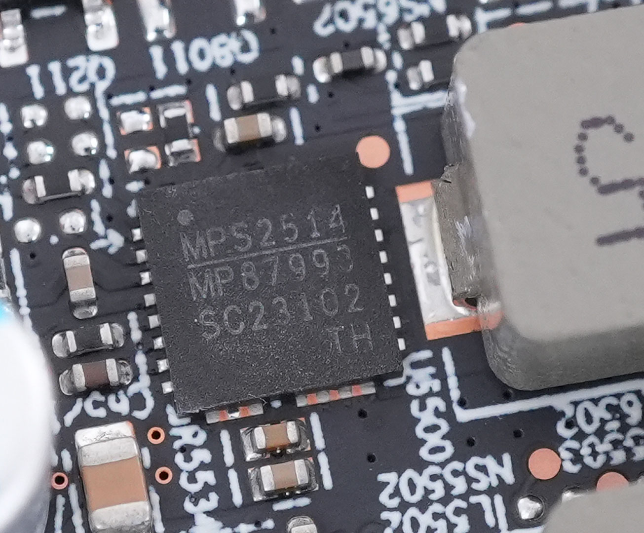
Just like GPU, the memory is handled by Monolithic MP87993 DrMOS chips.

The GDDR6 memory chips are made by Samsung, and bear the model number K4ZAF325BC-SC20, they are rated for 20 Gbps. This is the first RX 9060 XT with Samsung memory that we've tested, all the other cards we previously tested have Hynix memory.
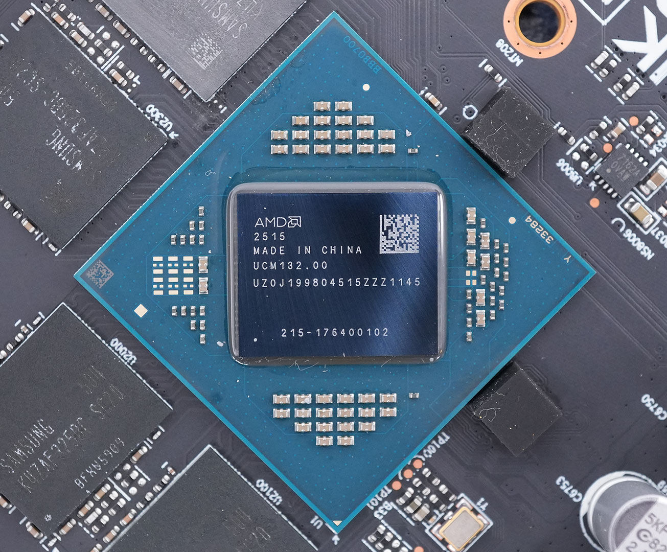
The AMD Navi 44 GPU at the heart of the Radeon RX 9060 XT is a monolithic die. It is fabricated using a 4 nanometer N4P process at TSMC Taiwan. The die measures 199 mm², and comes with a transistor count of 29.7 billion.
Nov 13th, 2026 22:12 CST
change timezone
Latest GPU Drivers
New Forum Posts
- What are you playing? (26214)
- Tell me about your favourite graphics card (30)
- no "PhysX" workable (8)
- AI generated images... (224)
- Crimson Desert (31)
- RenoDX HDR - how to view the differnce Before&After in game? (0)
- Displayport DP80 3M (10ft) cable that can achieve 80gbps stable? (5)
- I'll flash a ASUS ROG Strix RX480 O8G in Cause of Code 43, as a Newbie (1)
- Opinion on Monitor Replacement (6)
- TMOG - post your benchmark results here (16)
Popular Reviews
- AMD Zen 6 Technical Deep Dive
- Corsair HX1000i Shift Crystal Review
- NZXT C1200 Platinum Review
- Upcoming Hardware Launches 2027 (Updated Nov 2026)
- ASUS ROG Strix B850-I Gaming Wi-Fi7 W Review
- Montech King 95 3D PRO Review
- NZXT H7 RGB+ Review
- NZXT H5 Review
- Phantom Blade Zero Performance Benchmark Review - 35 GPUs Tested
- XPG NIMBUS PLUS Review - Mid-range Chair With Strong Competitors
TPU on YouTube
Controversial News Posts
- NVIDIA Co-Founder and CEO Jensen Huang Officially Resigns (379)
- OpenAI CEO Argues Home PCs Waste the World's Limited DRAM Supply (152)
- NVIDIA Launches Investigation Into Jensen Huang's Relationship With Suspected Chinese Spy (136)
- Intel "Raptor Lake Next" 16-Core and 20-Core CPUs Surface (130)
- Legendary Game Studio BioWare Shuts Down Following EA Layoffs (104)
- Dell CEO Says the Memory Shortage Will Get Worse in 2027 (95)
- NVIDIA GeForce RTX 50-Series Scheduled for up to $500 Price Hike This Week (89)
- Modder Fits RTX 5090 With Four 8-Pin Connectors, Halving Current per Wire (80)