 31
Silicon Motion MonTitan 7.68 TB Review
NVMe Power States »Teardown
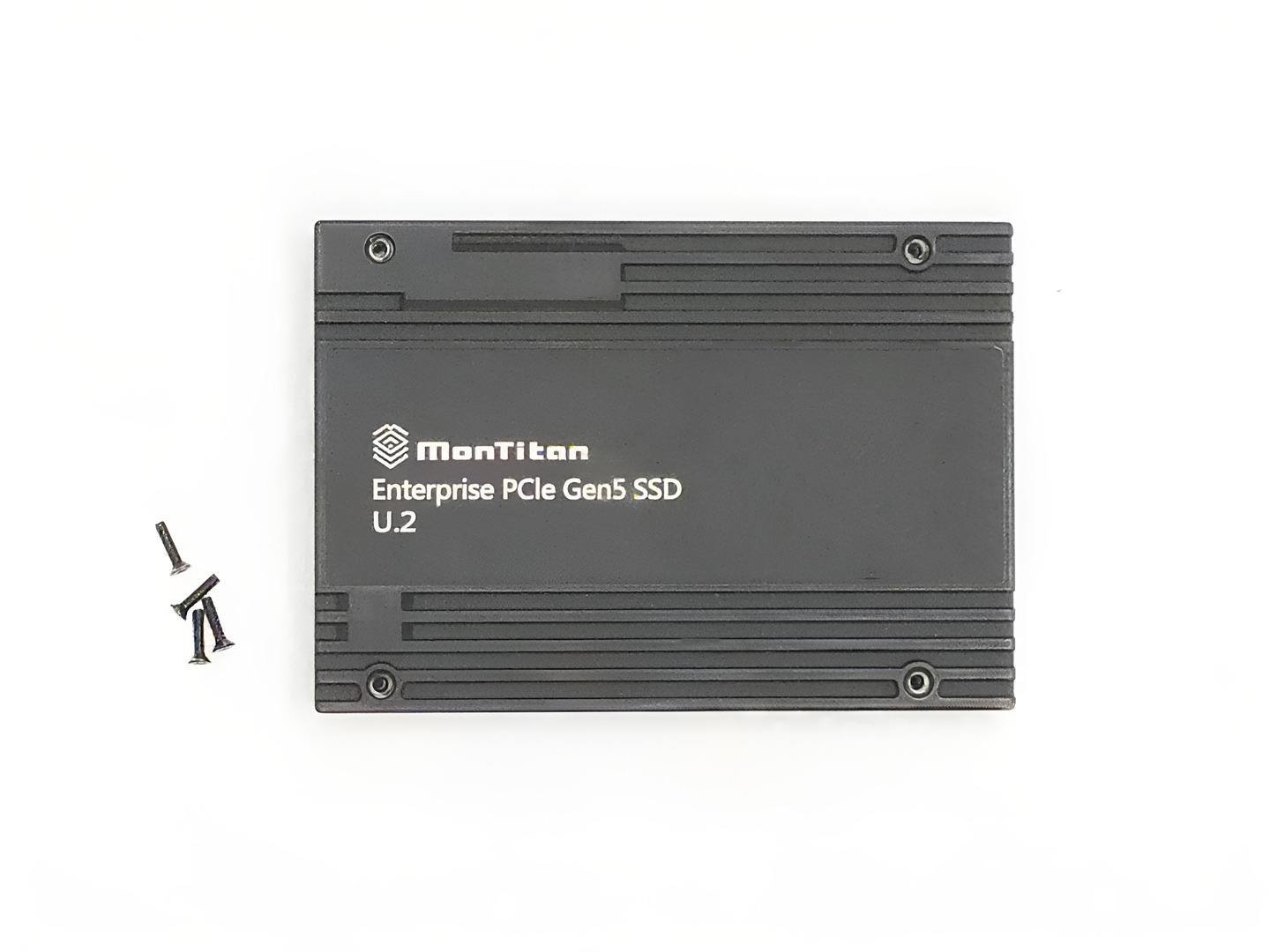
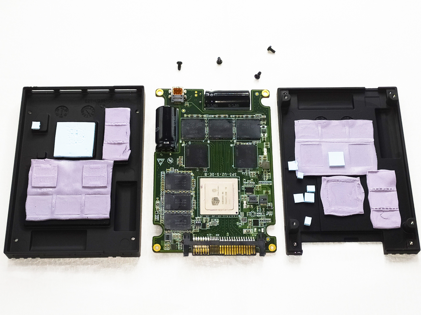
Upon opening the SSD, we see that it's secured with four Torx T-6 screws. Once removed, the front side of the PCB is revealed, firmly attached to the metal housing via several thermal pads that help dissipate heat from key components.


Next, after detaching the PCB from the enclosure, both sides of the board become visible, besides the interior of the metal casing. The opposite side is also lined with what appear to be high-performance thermal pads, further emphasizing the design's focus on effective cooling.
Controller
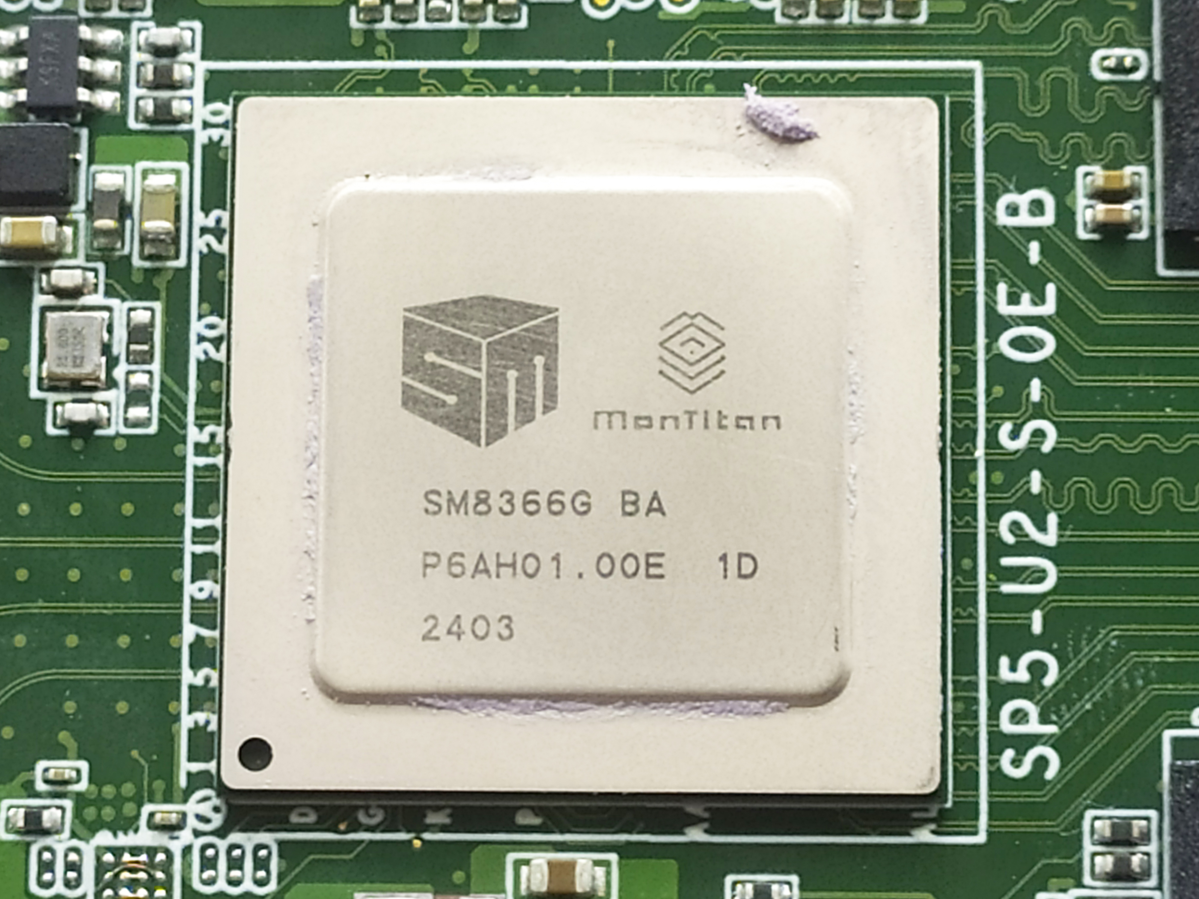
This MonTitan SSD lineup features Silicon Motion's new SM8366 Gen 5 enterprise controllers. Built on a 64-bit Arm architecture, the SM8366 integrates eight Cortex-A55 cores running at 1.4 GHz. It supports up to 16 NAND Flash channels with interface speeds of up to 2400 MT/s—enabling it to fully leverage the performance of nearly all modern NAND dies available today. The controller is also compatible with DRAM cache using DDR4 (up to 3200 MT/s) or DDR5 (up to 4800 MT/s), ensuring fast and efficient data handling.
The controller is manufactured using TSMC's well-known and widely adopted 12 nm FinFET process, offering a good balance between power efficiency and performance for enterprise-grade SSD applications.
It's interesting to see a Cortex-A series core like the 64-bit Arm Cortex-A55 used in an enterprise U.2 SSD controller, as most consumer-grade SSDs typically rely on real-time Cortex-R cores like the R5 or R8. The Cortex-A55, however, brings a higher level of processing power with out-of-order execution, a richer instruction set, and support for multithreaded operations. This makes it ideal for handling complex enterprise tasks such as advanced LDPC error correction, real-time telemetry, power management, and I/O coordination across many NAND channels. Its ability to support large DRAM caches, encryption, and workload balancing is crucial in data center environments where reliability, consistency, and scalability take priority over the alternative performance focuses of consumer drives.
The Cortex-A55 core isn't exclusive to enterprise hardware, it's also commonly found in smartphones and tablets. Designed for power efficiency and capable performance, it strikes a balance between low energy consumption and computational throughput, making it well-suited for mobile devices as well as high-end SSD controllers that demand both efficiency and parallel processing capabilities.
DRAM Cache
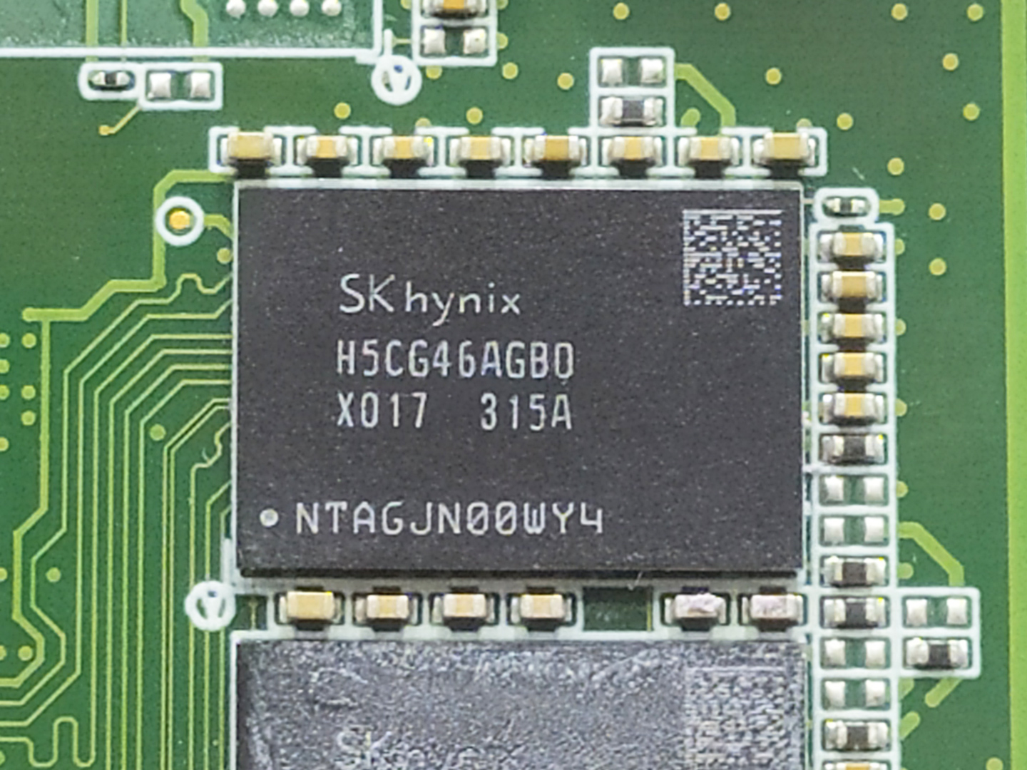
The SSD comes equipped with a total of six DDR5 chips from the South Korean manufacturer SK Hynix, with three modules on one side of the PCB and three more on the other side. The specific model used is the H5CG46AGBDX, each offering a density of 16 Gb (2 GB), adding up to a total of 12 GB of DRAM cache.
It's worth noting that not all of this memory is dedicated to storing the FTL (Flash Translation Layer) tables—it can also be allocated for ECC, which works by storing metadata and parity bits in DRAM to verify the integrity of user data before it's written to the NAND. This allows the controller to detect and correct bit errors in real time, to improve data reliability without adding extra stress to the flash itself.
NAND Flash
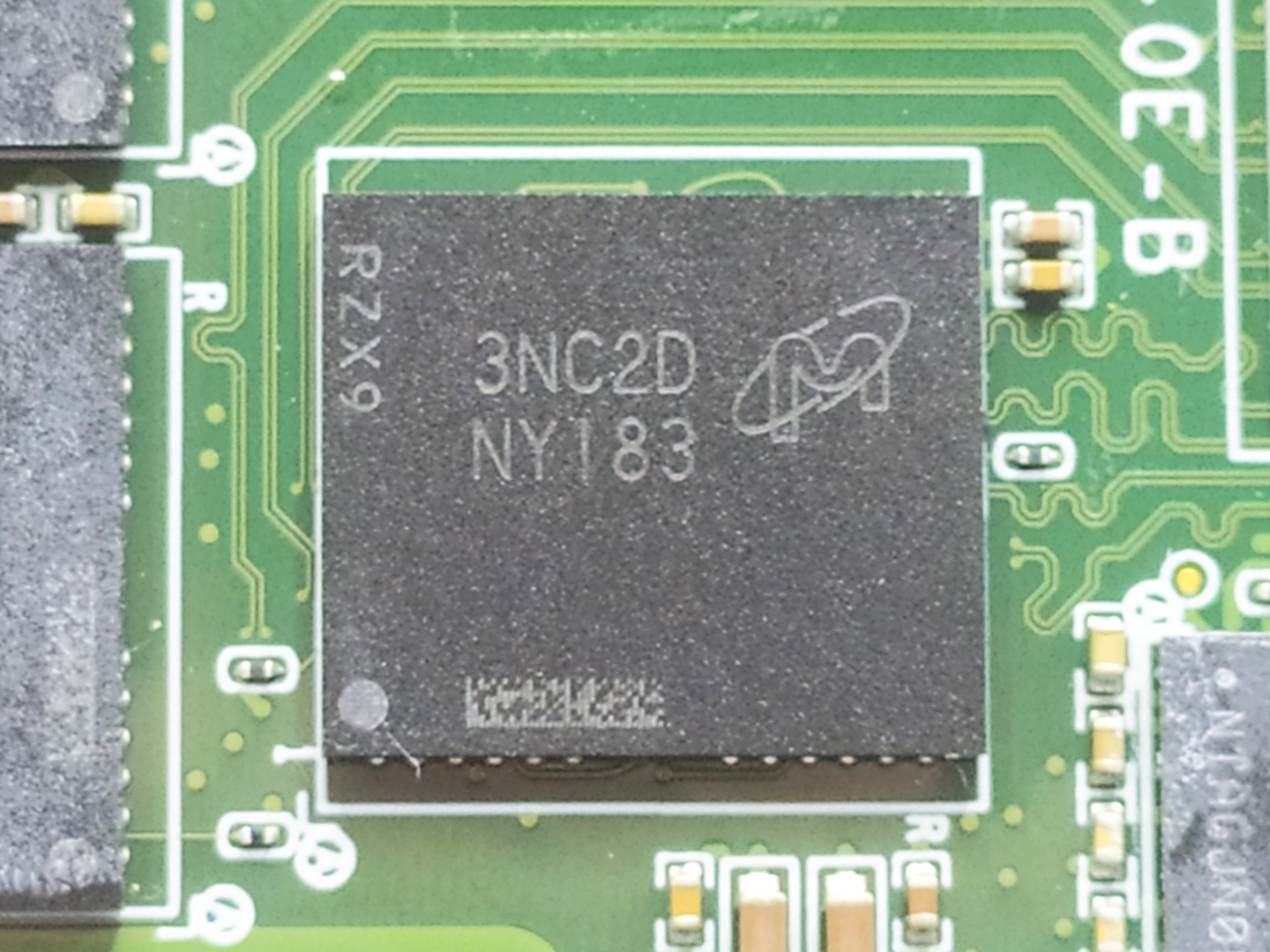
Our SSD features a total of 8 NAND packages, five on the top side of the PCB near the controller, plus three more modules on the bottom side, all supplied by the American manufacturer Micron. Using the manufacturer's own decoding tool, these "NY183" packages correspond to the NANDs MT29F8T08EULCHD5-T:C. The specific dies used are B58R FortisMax eTLC, with a density of 1 Tb per die and built using a 232-layer structure. Since the SSD includes 8 NAND packages and each die has a density of 128 GB (1 Tb), with 16 dies per package, each chip provides a total capacity of 1 TB (8 Tb).
These NANDs support ONFI 5.0 interfaces with speeds of up to 2400 MT/s. One of the key architectural upgrades contributing to their superior performance is the use of a 6-plane design, which significantly increases internal bandwidth compared to older-generation NAND.
Each die measures approximately 70 mm², resulting in a density of around 14.6 Gb/mm²—an impressive figure at the time of their release. Today, however, we're seeing newer TLC and even QLC dies reaching close to 20 Gb/mm², offering higher storage density in smaller die footprints.
Micron officially categorizes its NAND Flash into several product classes. The most commonly encountered are FortisMax and FortisFlash. FortisMax dies are typically designed for higher endurance and performance, making them ideal for datacenter and enterprise SSDs. FortisFlash, on the other hand, is more commonly found in consumer-grade drives.
There are other classifications, such as Mediagrade, which are similar to FortisFlash but generally offer lower endurance. Additionally, Micron operates a subsidiary called SpecTek, which sells NAND dies that didn't fully pass Micron's internal quality control processes. These SpecTek chips usually have reduced performance and durability compared to mainline Micron dies.
Structurally, the NAND uses a 2-deck configuration with 116 layers per deck, totaling 232 layers. However, the lower deck contains 127 gates, while the upper has one more, bringing the total to 253 gates. The design achieves an array efficiency of 91.7%, which reflects how much of the die's physical structure is utilized to store data. In this setup, the 253 gates represent all wordlines across both decks, while only 232 are actively used for storage (127 + 128 per deck). The remaining gates support redundancy, peripheral logic, and error correction. Higher array efficiency means less silicon is wasted, allowing better cost-effectiveness and potentially improved performance relative to die size.
VRM - Power Circuitry
Just like any other electronic component we use in our daily lives, SSDs require power in order to operate. Graphics cards, processors, and motherboards all have voltage regulators to supply power to their respective circuits—and the power delivery for SSDs works in the same way. In the next section of our analysis we'll take a closer look at these details.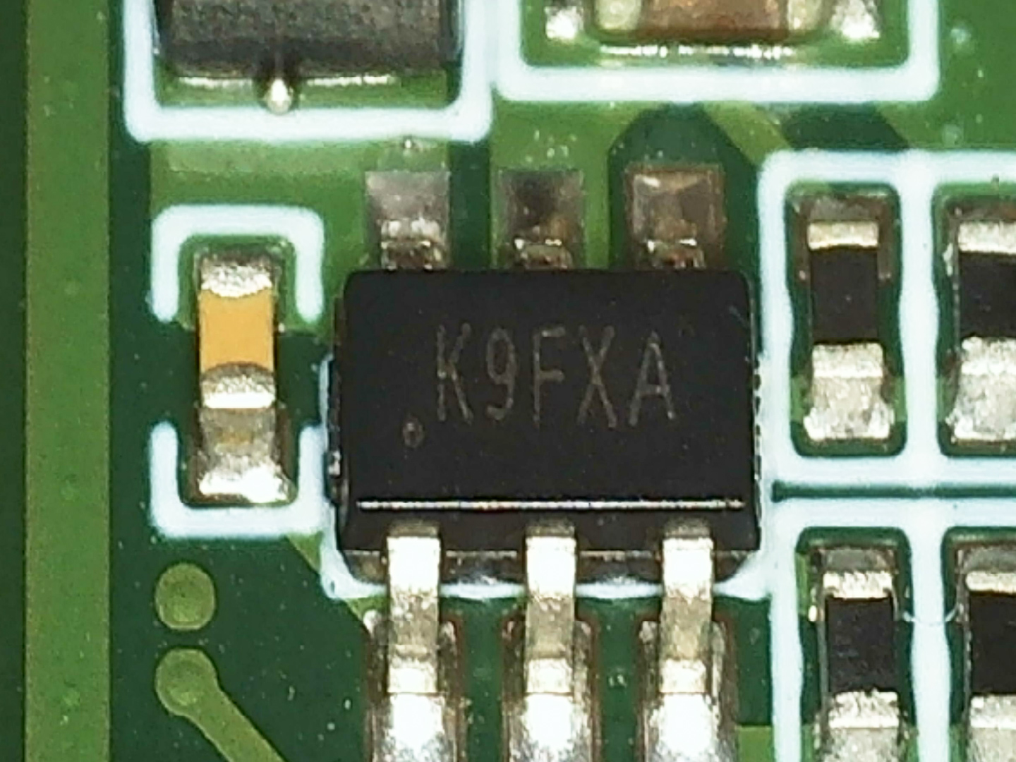
The first component, marked K9FXA, is a synchronous step-down regulator manufactured by Sylergy. It supports output currents of up to 2 A, operating within an input voltage range of 4.5 V to 18 V. Internally, it integrates two MOSFETs, one with a resistance of 130 mΩ and the other having 105 mΩ. Its thermal resistance is rated at 25 °C/W (junction-to-case), which is considered relatively high.
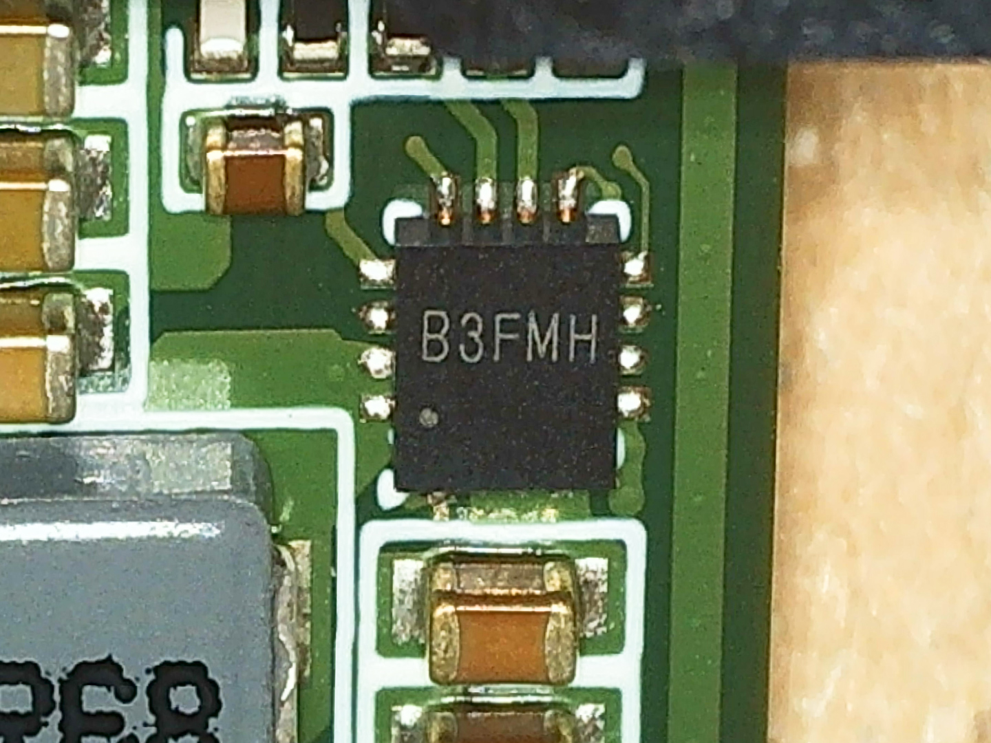
This other component is also a synchronous step-down regulator from Sylergy, but it is designed to handle significantly higher current up to 8 A. A notable characteristic is its much lower internal MOSFET resistance, rated at just 10 mΩ and 20 mΩ. This greatly improves efficiency and thermal performance, reflected in its thermal resistance of only 5.5 °C/W, a substantial improvement over the previous regulator.
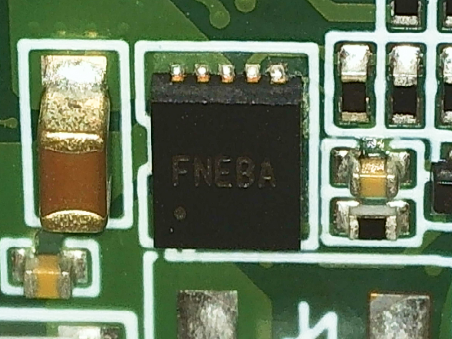
The other component, marked as FNEBA' is a Programmable Current Limit Switch with an OVP (Over-Voltage Protection) clamp, designed for current control as its name suggests. Manufactured by Sylergy, it integrates a low-resistance 40 mΩ N-channel MOSFET and supports operating voltages up to 15 V. It is rated for a maximum power dissipation of 2.6 W with a Junction-to-Case thermal resistance of 8 °C/W.
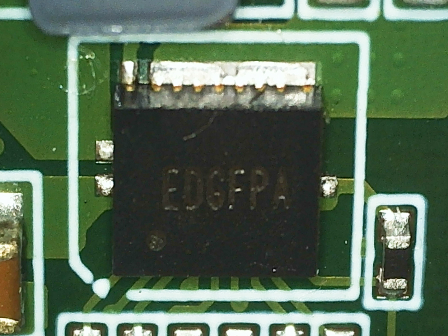
Lastly, we have another Sylergy component, marked EDGFPA' which is a high-efficiency synchronous step-down regulator. Designed to deliver up to 20 A of continuous output current, it operates across a wide input voltage range of 2.9 V to 16 V. The output voltage can be configured between 0.6 V and 5.5 V, making it versatile for powering different parts of the SSD circuitry. With integrated power and rectifier switches, it achieves high efficiency while minimizing board space.
There are several other smaller components in this SSD's design, but unfortunately I was only able to gather information on the ones mentioned above.
Power Loss Protection
Power loss protection in datacenter SSDs is essential to ensure data integrity during power failures. Using capacitors for temporary energy storage allows the safe completion of ongoing operations, preventing data corruption in critical environments. This ensures high availability and reliability of data.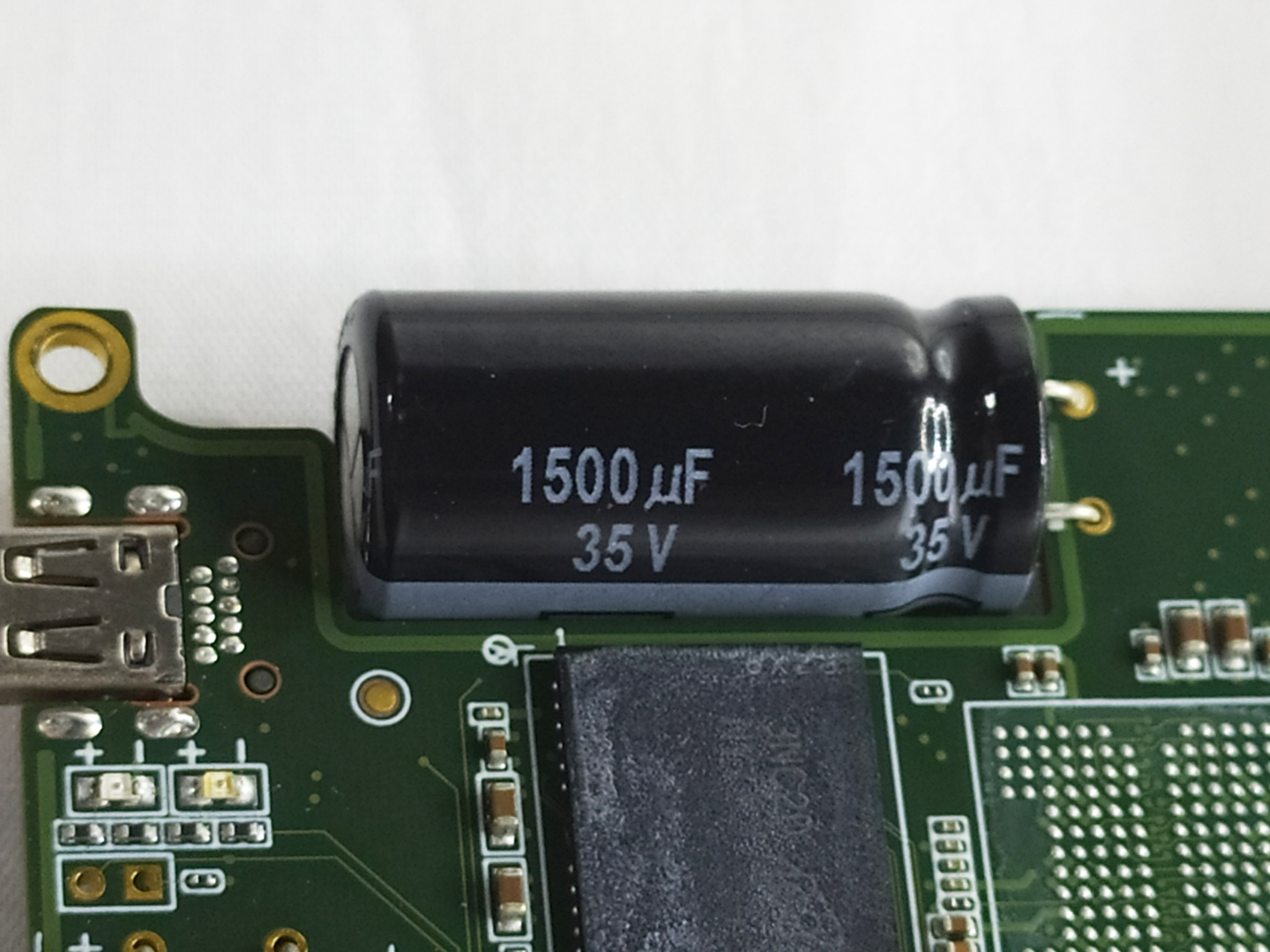
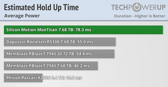
This design incorporates two 1500 µF electrolytic capacitors, rated at 35 V and specified to operate at temperatures up to 105°C.
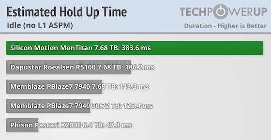
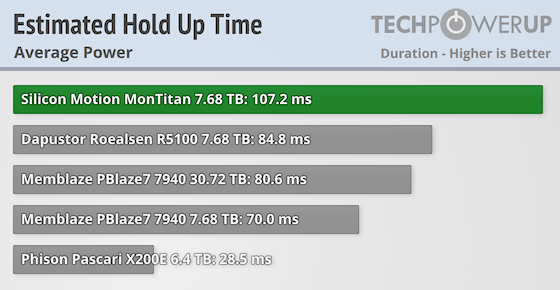
Estimated Hold Up Time
To estimate the hold-up time, we applied a set of equations that help approximate how long the drive can remain operational during an unexpected shutdown, based on its energy requirements. Our calculations use measured values for idle, average, and peak consumption. The analysis also considers the number and size of onboard capacitors, along with specific energy usage under various workload conditions.Please note: It's important to note that it's not an exact measurement, but rather a simplified calculation to illustrate how long an SSD might remain powered during a sudden power loss. In real-world conditions, power consumption is typically lower than the scenario shown here, which would result in a longer hold-up time.
Nov 22nd, 2026 11:13 CST
change timezone
Latest GPU Drivers
New Forum Posts
- Zen 3 IF/IMC degradation (245)
- Ryzen or Intel system (21)
- Honestly, do you care about GTA VI? (252)
- Your PC ATM (36452)
- The TPU UK Clubhouse (27291)
- Can you guess Which game it is? (346)
- Making a game in Godot engine (17)
- TPU's Nostalgic Hardware Club (22197)
- Intel D270 (1)
- Gigabyte AORUS RTX 5080 MASTER – Up to 30°C GPU Hotspot Delta! Is This Normal, a Cooling Defect, or Should I RMA? (14)
Popular Reviews
- Microsoft Surface Laptop Ultra Review - The Next-gen Arm Laptop
- Corsair RM1200e (Second Generation) Review
- Pulsar Office Tour & First Look at P1 Dual-Sensor Mouse
- Upcoming Hardware Launches 2027 (Updated Nov 2026)
- Ugreen NASync DXP4800 GT Review
- AMD Ryzen 7 9800X3D Review - The Best Gaming Processor
- Biwin Black Opal NV7400 2 TB Review
- AMD Zen 6 Technical Deep Dive
- Phantom Blade Zero Performance Benchmark Review - 35 GPUs Tested
- AMD Ryzen 7 5800X3D 10th Anniversary Review
TPU on YouTube
Controversial News Posts
- NVIDIA Co-Founder and CEO Jensen Huang Officially Resigns (492)
- Report: Jensen Huang Eyes NVIDIA Comeback (263)
- Open Letter Asking NVIDIA to Reinstate Jensen Huang Passes 115,000 Signatures (184)
- OpenAI CEO Argues Home PCs Waste the World's Limited DRAM Supply (152)
- NVIDIA Launches Investigation Into Jensen Huang's Relationship With Suspected Chinese Spy (136)
- Intel "Raptor Lake Next" 16-Core and 20-Core CPUs Surface (130)
- NVIDIA GeForce RTX 50-Series Scheduled for up to $500 Price Hike This Week (89)
- Intel Razor Lake Gets a 12 P-Core bLLC Chip With No E-Cores, Per Leak (86)