 16
16
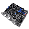
Gigabyte GA-X79-UD5 Intel LGA 2011 Review
BIOS Walkthrough »The Board - A Closer Look


Up in the top-right corner of the Gigabyte GA-X79-UD5 we find a bright red, high quality ON/OFF switch as shown in the first image above, one that closely resembles the TPU logo you see in your browser tabs. It's in a slightly weird location, all the way up at the top, made even more puzzling by the fact that the RESET switch is found on the bottom right of the board, shown in the second picture above. This layout is actually pretty useful to those that use open-air test benches, as more often than not, the right edge is what faces the front of a test bench. ON/OFF on one side, and RESET on the other makes sense in this situation, but otherwise, it's actually quite inconvenient. However, it also hints that this board was made to be put into a test bench as used for overclocking, but we would have much prefered to have the RESET and ON/OFF switches close together, even if both are way up at the top like the ON/OFF button is here.
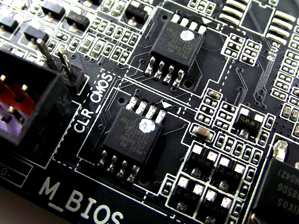

The BIOS solution that Gigabyte provides is actually rather complex, but we prefer to think of it as a highly refined "Dual BIOS" implementation that Gigabyte has been providing for at least a decade. Using dual matched Macronix 64 Mb ROMs as shown in the first image above, the Gigabyte GA-X79-UD5 features one of the most functional hardware BIOS solutions we've ever seen, primarily controlled via the buttons on the back panel seen in the second image above. The lower button, as non-descript as it is, allows users to chose which Macronix ROM they are booting from, allowing a quick and easy way to swap between stock and overclocked profiles, or for easy recovery from a failed boot due to improper settings when overclocking. Beyond you pushing the button in to activate the back-up ROM, the board itself will automatically switch to the backup ROM itself after several failed boots, and if the main BIOS becomes corrupted, the board will automatically flash a new working copy from the back-up ROM, too. Pushing the "O.C." button will enable an automatic system overclock while at the same time enabling the XMP v1.2/v1.3 memory profile, if your DIMMs support either version.
This is the first time that Gigabyte has provided such an easy way to make use of the multiple BIOS ROMs that they have been shipping on countless products, for years and years. It's simple and easy to use, still provides the same functionality that previous iterations have, and then some, while finally providing the end user with a choice that really expands overall functionality of the entire product, something that goes a long way for those that like to benchmark and push their system to the limit.
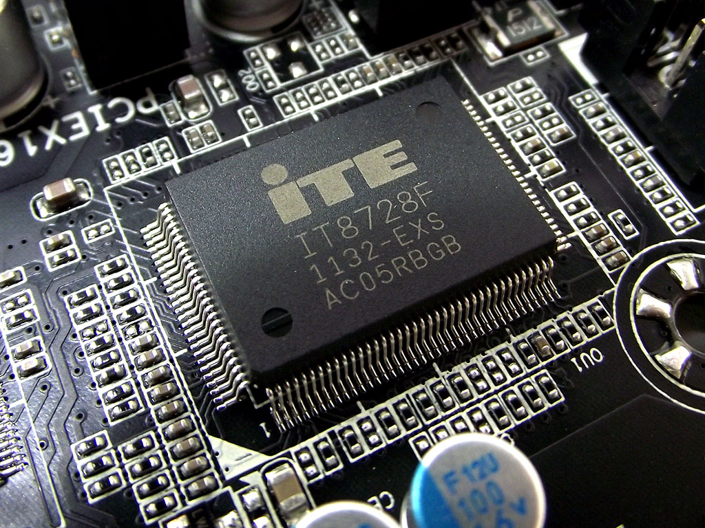
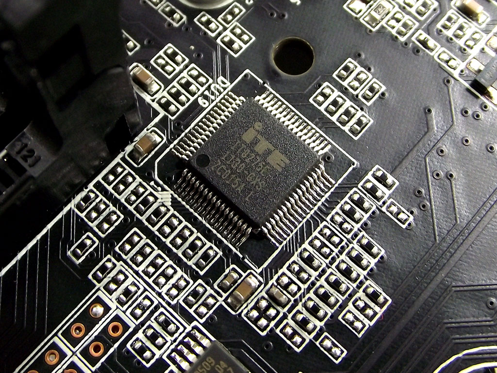
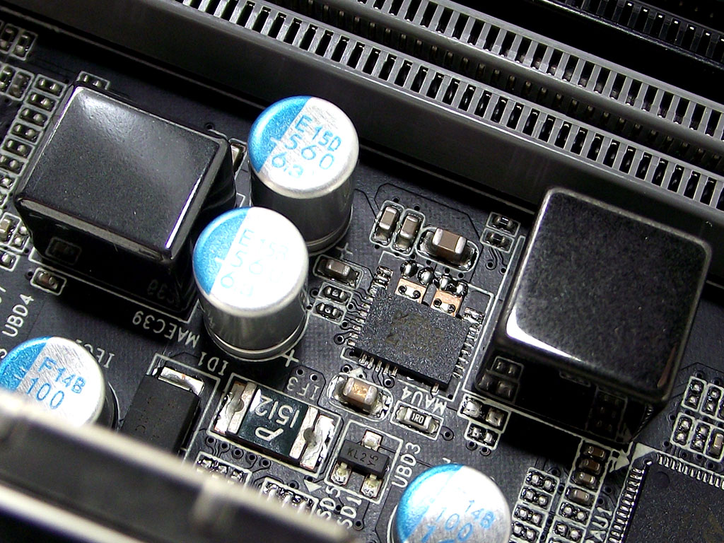
System monitoring functionality is provided by an ITE IT8728F, a chip we've seen before a few times now, responsible for sensor data monitoring and fan control. The primary voltage controller is another ITE part, and IT8275E, which was also on the G.1 Sniper2 we reviewed quite some time ago. The ITE IT8275E serves as the "brain" of the VRM system, providing voltage monitoring and calibration, reading back data from the other three phase controllers.
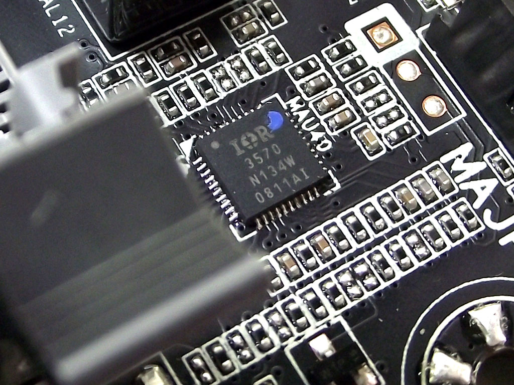

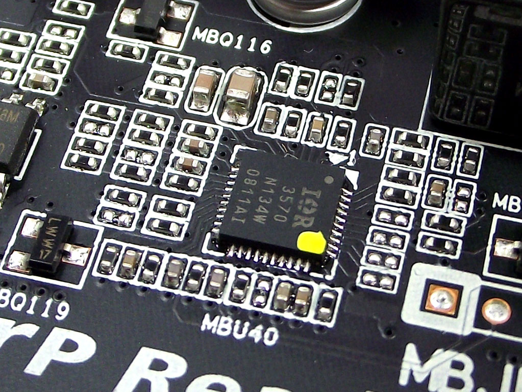
Those other three controllers are provided by International Rectifier, seen in the three images above. From left to right, as they appear above, they appear on the board itself, with the IR3570 seen in the first image next to the left DIMM bank; in the middle is the IR3567 responsible for the CPU, and on the right we have the IR3570 that controls the right DIMM bank. All three are digital controllers that not only allow voltage to be set, but also the OCP limits, and frequency that the individual VRM sections refresh at as well as V-Droop control. Together they make a pretty powerful and highly customizable solution that can very neatly meet the needs of even the most extreme users. We mentioned earlier that this board was built for overclocking, and this is yet another indicator that there might be more to this board than first meets the eye.
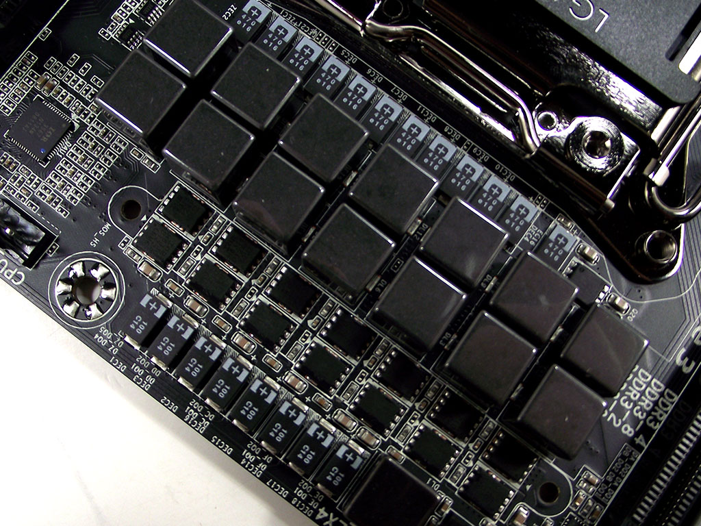

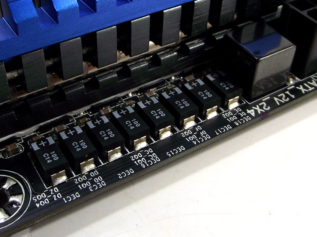
The X79-UD5 features a standard hi/low VRM design with 14 total phases for the CPU itself. There are a total of ten phases dedicated to the CPU cores, pushed with five dual-channel input drivers that are found on the rear of the motherboard. The other four phases are for the System Agent and VTT domains, each in a pair with their own dual-channel input driver that is hidden under the VRM heatsink behind the EPS 8-pin connector. It's worth noting that the input drivers are balanced with several surface-mounted capacitors on the front side of the board, seen in the third image above. It's not often we see capacitors on both the input and output stages, but this new all-digital VRM design from International Rectifier that Gigabyte employs on the GA-X79-UD5 is pretty robust, that when combined with the DIMM VRMs, offers a level of customization not seen outside of Gigabyte's Intel X79 Express products.

The above two pictures show the two DIMM VRMs, the first image showing the VRM for the right bank, and the second showing the VRM for the left bank. Each VRM section is located as close as possible to the DIMMs they power, in order to eliminate line noise and line interference from other onboard parts. Each phase for the DIMM VRMs has its own input driver and high/low MOSFETs, as well as chokes, capacitor, and controller. It appears as though perhaps the DIMM phases could have been a bit more robust, with an area under and next to the hex-FET that appears to have been designed to hold a larger component. We'll have to investigate the memory clocking situation later.

The PCIe subsystem is very basic. Each of the PCIe slots is directly connected to the CPU, with only the ICS 9FGL1214AKLF clock buffer seen in the image above as an outside component. With all of the LGA 2011 CPUs supporting 40 total PCIe lanes, there is no need for switches or anything else with just three PCIe slots, two with x16 links, and the third with a x8 link.
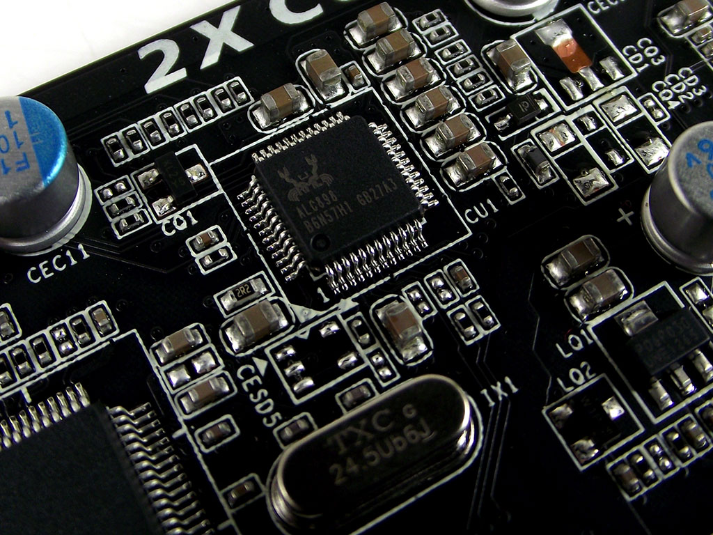

The included Realtek ALC898 HD codec supports 7.1 audio, and meets Microsoft's WLP3.x audio requirements. Supporting 44.1k/48k/96k/192 kHz sampling at 16-, 20- and 24-bit, the Realtek ALC8989 includes full support for HD audio formats featuring Content Protection, if supporting software is used. It is also DirectSound 3D compatible, so no area of usage or functionality is overlooked, including support for Dolby Home Theatre. Gigabyte has sourced the LAN controller for the GA-X79-UD5 from Intel, fitting the GA-X79-UD5 with the Intel 82579V which meets the 802.3az Energy Efficient Ethernet appliance standard.


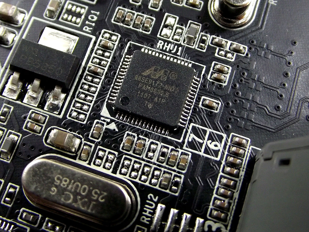
For extra drive support via the eSATA and internal SATA ports, Gigabyte has equipped the GA-X79-UD5 with no less than three Marvell 88SE9172 controllers, with the one in the first image above powering the extra two eSATA 6 Gb/s ports, and the other two controllers, in the second and third images, manage the grey internal SATA 6 Gb/s ports found on the right board edge. All of the Marvell controllers support RAID 0 and RAID 1.

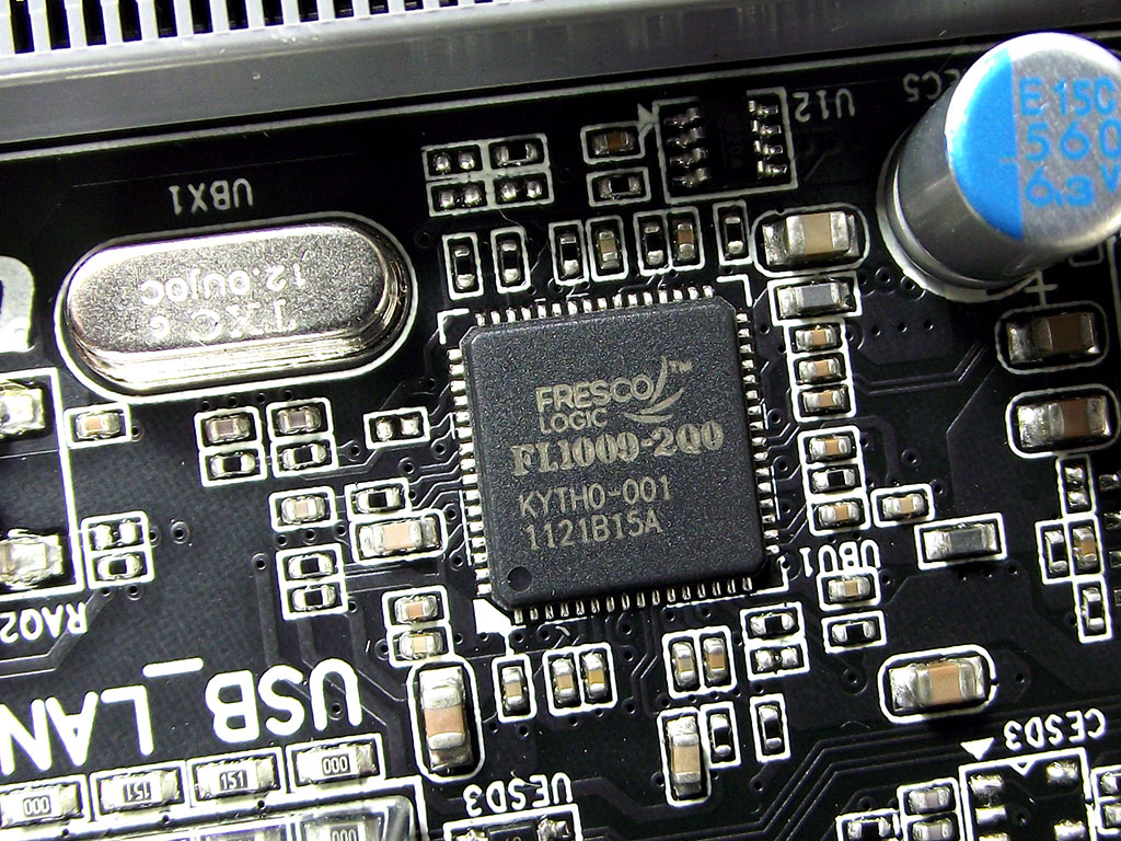
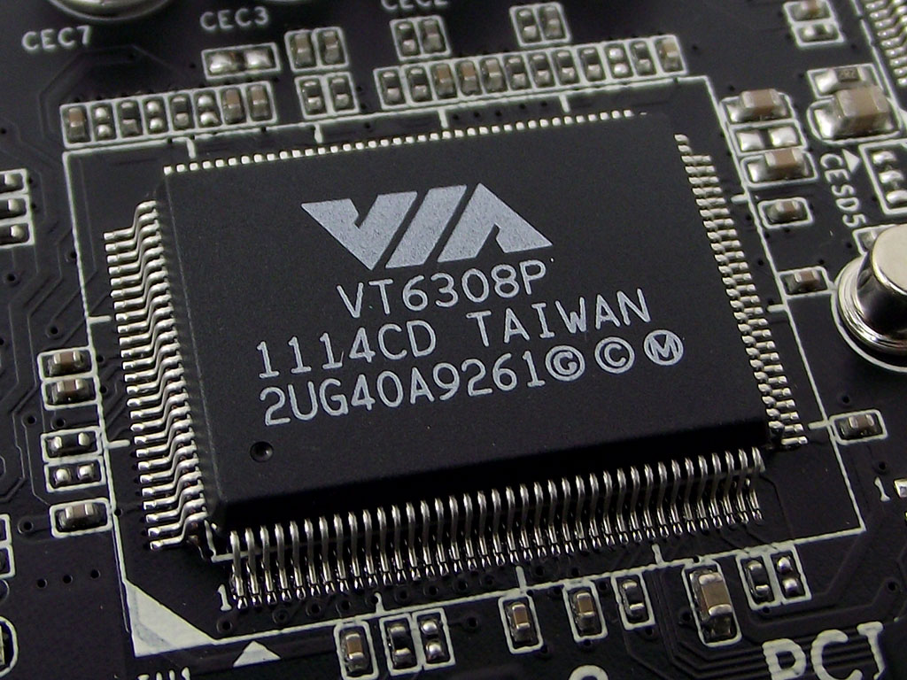
For USB 3.0 support, we find dual FrescoFL1009-2Q0 PCIe controllers, one for the internal header that provides USB 3.0 to casing front panels, and one for the ports on the rear. The VIA VT6308P in the third image above provides the GA-X79-UD5's IEEE 1394 FireWire support, powering both the port on the rear I/O as well as the internal header found on the board's bottom edge.


The Gigabyte GA-X79-UD5 includes a separate Bluetooth 4.0 and WiFi card that uses both the PCIe bus, as well as USB 2.0. The two separate devices occupy the same card, but feature separate antennas and interfaces. Because only one USB 2.0 port is used, the card has a USB 2.0 port built on it, but we're not exactly sure why, as it is not the sort of port that can be wired to the case exterior, but rather a normal USB 2.0 port you might plug your keyboard or mouse into. It's nice to have access to the unused port, but it could have been provided in a slightly better way, like perhaps sticking out the same end as the antenna receptacles.


With all the heatsinks removed, we can easily see the heatpipe that joins them. We were actually quite surprised to find that looking at the cooler like this made the VRM portion seem so small, and small it is. The piece that sits on the Intel X79 express chipset seems to actually do most of the cooling, making us wonder if there could not have been a more effective solution, however, under high load testing we found the cooler to do a more than adequate job, as we noticed no throttling at any point, even when pushing 280 W through the EPS 8-pin.
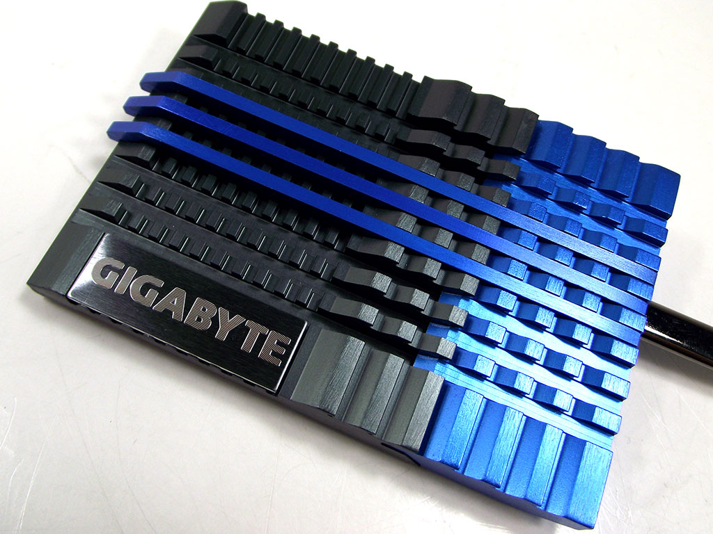
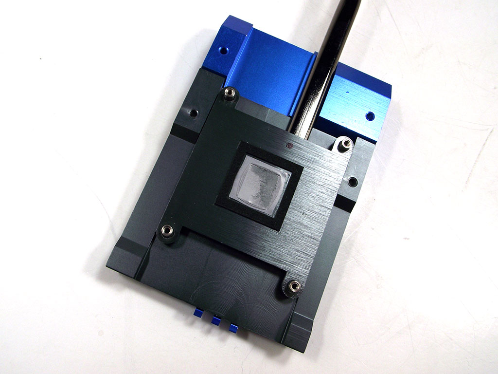
Looking closer at the southbridge cooler we can see that it is composed of two separate pieces of metal that have been machined to increase surface area, and then anodized. From below we can see the contact area that the Intel X79 Express chipset comes into contact with, with the heatpipe from the VRM cooler passing over just one side where the chipset would be, like we saw on the ECS X79R-AX.

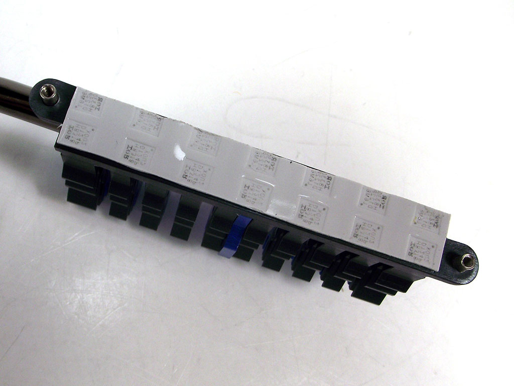
The VRM cooler, as we mentioned, is quite small, and like the southbridge cooler, is also made up of two anodized pieces of aluminum. Looking at the contact pad we can see very distinct impressions made by the International Rectifier hexFETs, so while the cooler is small in size, it definitely makes good contact with the parts that need cooling.

In the above picture you can clearly see the new Intel X79 Express chipset, found under the large southbridge cooler. The chip itself is fairly large, and while we are used to seeing the Intel X79 Express chipset surrounded by a complex array of surface mounted bits on the board itself, the Gigabyte GA-X79-UD5 seems to provide a much more simple assembly.
Apr 26th, 2024 14:27 EDT
change timezone
Latest GPU Drivers
New Forum Posts
- looking to build a new system and im considering asrock brand but i have some doubts/concerns. (0)
- What phone you use as your daily driver? And, a discussion of them. (1485)
- XFX RX470 8GB no video and error 43 (29)
- DTS:X APO4 + DTS Interactive for Most Devices [USB Supported] (305)
- The Official Linux/Unix Desktop Screenshots Megathread (702)
- What's your latest tech purchase? (20352)
- hacked (73)
- im new to throttelstop and i think i messed it up by copying others any hints would be very much aprreciated (5)
- 2022-X58/1366 PIN Motherboards NVME M.2 SSD BIOS MOD Collection (657)
- DTS DCH Driver for Realtek HDA [DTS:X APO4 + DTS Interactive] (1909)
Popular Reviews
- HYTE THICC Q60 240 mm AIO Review
- MOONDROP x Crinacle DUSK In-Ear Monitors Review - The Last 5%
- Alienware Pro Wireless Gaming Keyboard Review
- Upcoming Hardware Launches 2023 (Updated Feb 2024)
- Thermalright Phantom Spirit 120 EVO Review
- FiiO K19 Desktop DAC/Headphone Amplifier Review
- ASUS Radeon RX 7900 GRE TUF OC Review
- AMD Ryzen 7 7800X3D Review - The Best Gaming CPU
- RTX 4090 & 53 Games: Ryzen 7 5800X vs Ryzen 7 5800X3D Review
- NVIDIA RTX 4090: 450 W vs 600 W 12VHPWR - Is there any notable performance difference?
Controversial News Posts
- Windows 11 Now Officially Adware as Microsoft Embeds Ads in the Start Menu (129)
- Sony PlayStation 5 Pro Specifications Confirmed, Console Arrives Before Holidays (117)
- NVIDIA Points Intel Raptor Lake CPU Users to Get Help from Intel Amid System Instability Issues (106)
- AMD "Strix Halo" Zen 5 Mobile Processor Pictured: Chiplet-based, Uses 256-bit LPDDR5X (103)
- US Government Wants Nuclear Plants to Offload AI Data Center Expansion (98)
- AMD's RDNA 4 GPUs Could Stick with 18 Gbps GDDR6 Memory (93)
- Developers of Outpost Infinity Siege Recommend Underclocking i9-13900K and i9-14900K for Stability on Machines with RTX 4090 (85)
- Windows 10 Security Updates to Cost $61 After 2025, $427 by 2028 (84)