Thursday, September 17th 2015

NVIDIA "Pascal" GPUs to be Built on 16 nm TSMC FinFET Node
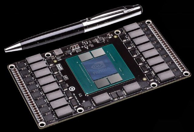
NVIDIA's next-generation GPUs, based on the company's "Pascal" architecture, will be reportedly built on the 16 nanometer FinFET node at TSMC, and not the previously reported 14 nm FinFET node at Samsung. Talks of foundry partnership between NVIDIA and Samsung didn't succeed, and the GPU maker decided to revert to TSMC. The "Pascal" family of GPUs will see NVIDIA adopt HBM2 (high-bandwidth memory 2), with stacked DRAM chips sitting alongside the GPU die, on a multi-chip module, similar to AMD's pioneering "Fiji" GPU. Rival AMD, on the other hand, could build its next-generation GCNxt GPUs on 14 nm FinFET process being refined by GlobalFoundries.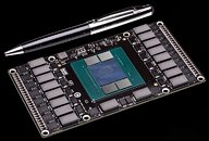
Source:
BusinessKorea
52 Comments on NVIDIA "Pascal" GPUs to be Built on 16 nm TSMC FinFET Node
I just hope GloFo and TSMC deliver what was promised on schedule. AMD especially has their continued existence riding on GloFo delivering.
If AMD got 14nm over NVidia's 16nm, that would be relatively hilarious.
Assuming both do deliver, yeah, it's pretty funny that AMD will have a process advantage over NVIDIA. Personally, I think I would be planning and placing orders for both. Both failing seems pretty remote so in either case, they wouldn't be completely left out to dry. I wonder if NVIDIA even considered GloFo or are they so prideful they consider doing so beneath them?
Nvidia hasent gone down that way yet or at least as we know of, so they are still in the learning process. Now they have teamed up with TSMC again, the manufacturer that hasent done anything regarding HBM yet, to me thats a big gamble.
1 thing is to make the tec work, another is to make it work "perfect" and for me AMD has the upperhand here, since both AMD and Samsung allready has the working process going and finetune it.
More than likely nVidia pulled a nVidia and demanded more than it was worth for Samsung. They did the same thing to Microsoft on the Xbox and then again to Sony on the PS3. Was no surprise no one would deal with their chips in consoles after that.
2. TSMC don't assemble the package. TSMC supply the GPU silicon. Hynix (or Samsung) supply the HBM IC's and interposer silicon, and in the case of AMD's Fury, another third party, Amkor, assembles the package.If history tells us anything, it is that both camps tend to be very close on timetable and performance. R&D commitment is the key going forwardGloFo is perpetually behind schedule- partly from their way too optimistic timetables. If GloFo kept to their word, they would have been pumping out 14nm XM silicon since mid 2014. FWIW, both Samsung and TSMC are at least a quarter behind in their schedule. The only difference is, TSMC hasn't had their business contracts cut because of bad yields by all accounts.Yes this makes perfect sense. :rolleyes: More likely is that risk silicon is showing which process is better suited to getting the parts out on time and at the performance parameters required ( I also wouldn't be surprised to see AMD follow suit on the large chips).
The real unknown for this generation is how much more computing power will be unleashed by moving from 28 to 16 or 14nm. This 22nm blunder hurt everyone and kept both and Nvidia and AMD rehashing old designs. (I know, Nvidia worked some magic towards power consumption, but isn't very relevant on a desktop and came at the cost of gimped computing power - a worthwhile cost for many, but still a cost).
I doubt we will see a huge performance increase with 14/16nm.....with cards being at best 50% faster than current gen, even 30% wouldnt surprise me...........at least for first gen cards. AMD and Nvidia will leave a little in the tank for a refresh.
The biggest jump on past process nodes is like 75%, and most are usually much less. The aim for them is to keep us buying upgrades.
Where my interest lies is strictly in a gaming card and I expect a single Flagship Pascal to be able to handle 4K at 60 FPS in just about every game. The midrange Pascal should be faster than a 980 Ti and an entry level Pascal should be able to handle almost every game at 1080p at 60 FPS. I think for people expecting an increase in performance like we got with Maxwell over Kepler will be in for a pleasant surprise. I'm expecting a much larger increase in performance from Pascal over Maxwell.
TSMC have already stated that 16nmFF+ has twice the transistor density as a comparable 28nm IC, so if big Pascal is (for arguments sake) ~ 16bn transistors, then it is comparable in size to GM200 at 8bn transistors - ballpark*
*Uncore ( I/O, command processor, memory controllers, cache, transcode engine etc.) has a lower transistor density than the shader core, so any calculation needs to take into account the reduced uncore (due to the reduction in size of HBM's memory control in relation to that of GDDR5 IMC's).AMD may have first option on Hynix's HBM2, but I doubt that they have a lock on Samsung's as well.
Anyway, Pascal is probably 12 months away. Until then many things can happen. TSMC does have the advantage of experience over Samsung and I am not sure how good Samsung's process will be for big GPUs that eat 200W TDP and not just small SOCs that can be happy with 4-5W TDP.
uhm... there shouldn't be any reason for nvidia not to use GDDR5 for their entry level cards. Hell, even for some of the mid range.
i dont want a GTX 750 ti esque card to cost 200$
Don't forget that GloFo has a partnership and technology agreement with Samsung and that is how GloFo got 14nm FinFET. It will be interesting what the next couple years will bring...
I just noticed that remark about the non-traditional scaling with 28nm to 14nm/16nm and that they aren't really true 14nm or 16nm but something between that and 20nm. >_<
So, that was pointless on my part.
It could also allow cards like the 960 to return to a single-slot design, as opposed to the current dual slot design, along with gpu power consumption taking another dip. I'd love to have my 770s performance in a sub 100 watt gpu. And, if hbm2 is only used on high end chips, the price of hbm will fall much more slowly than if it is used everywhere.