Thursday, May 20th 2021

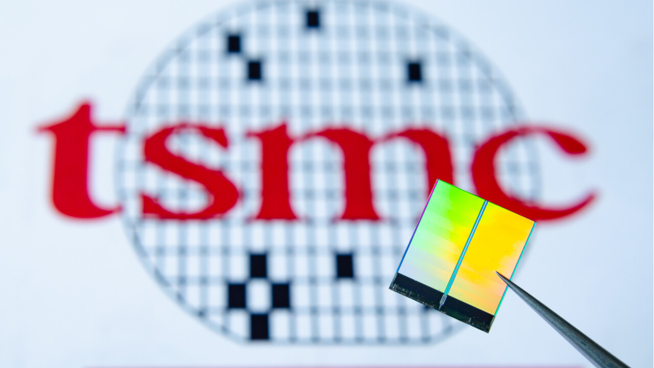
TSMC Claims Breakthrough on 1nm Chip Production
TSMC in collaboration with the National Taiwan University (NTU) and the Massachusetts Institute of Technology (MIT) have made a significant breakthrough in the development of 1-nanometer chips. The joint announcement comes after IBM earlier this month published news of their 2-nanometer chip development. The researchers found that the use of semi-metal bismuth (Bi) as contact electrodes for the 2D matrix can greatly reduce resistance and increase current. This discovery was first made by the MIT team before then being further refined by TSMC and NTU which will increase energy efficiency and performance in future processors. The 1-nanometer node won't be deployed for several years with TSMC planning to start 3-nanometer production in H2 2022.
Source:
Nature
35 Comments on TSMC Claims Breakthrough on 1nm Chip Production
How is that even a thing?
Thanks for the article! gives hope for the future of semiconductors.
Putting 'nm numbers' on things like FinFETs, GAA FETs and whatever else they're cooking up doesn't really make all that much sense anymore anyway, and as technologies continue to develop it's less and less about those nanometers.
If only there was something else both straightforward and catchy that can represent both performance and scaling of the most basic building blocks of transistors these days,..
Edit: It makes me think of those oldskool "3200+" names AMD put on their CPUs when clocks started to matter less compared to IPC. It's not really a straightforward metaphor but similar imho.
Prior to FinFET, 3D gates weren't present. Actual 3D gates in the shape of GAAFET and MBCFET are 4D in comparison since the gate is surrounding the source in 4 directions instead of 3.
If anything it says to me that the products are too cheap for their demand so people are capitalizing on the difference. If supply and demand were in balance, scalpers shouldn't have a chance.
In all seriousness, I wonder what this means for CPUs and GPUs. Will this drive safe voltages down, up, or something else?
In both case, the major issue will be the cooling. This is why 3d stacking is targeted right now at low power devices. But all manufacturer are working on solutions for that.
Now we are in the same position and so far the proven ways to get us under 5nm has been Nanosheet or Nanowire (Gate all-around) FETs. Its all about how to control the channel effectively and not allow electrons to leak from source to drain even if the FET is technically off. FINFET has a lot better control over channel behavior, but as the transistors get smaller we run into same problems exhibited by normal planar FETs when first trying to get below 22nm.
You are dead on about manufacturing though, going to FINFET was hell and a half for the industry due to tight tolerances to how FINFETs function. Nanosheet and wire solutions are even more difficult. Costs is going to be insane.
This new contact material is pretty interesting actually. Might add a bit to manufacturing costs though.