Thursday, May 20th 2021

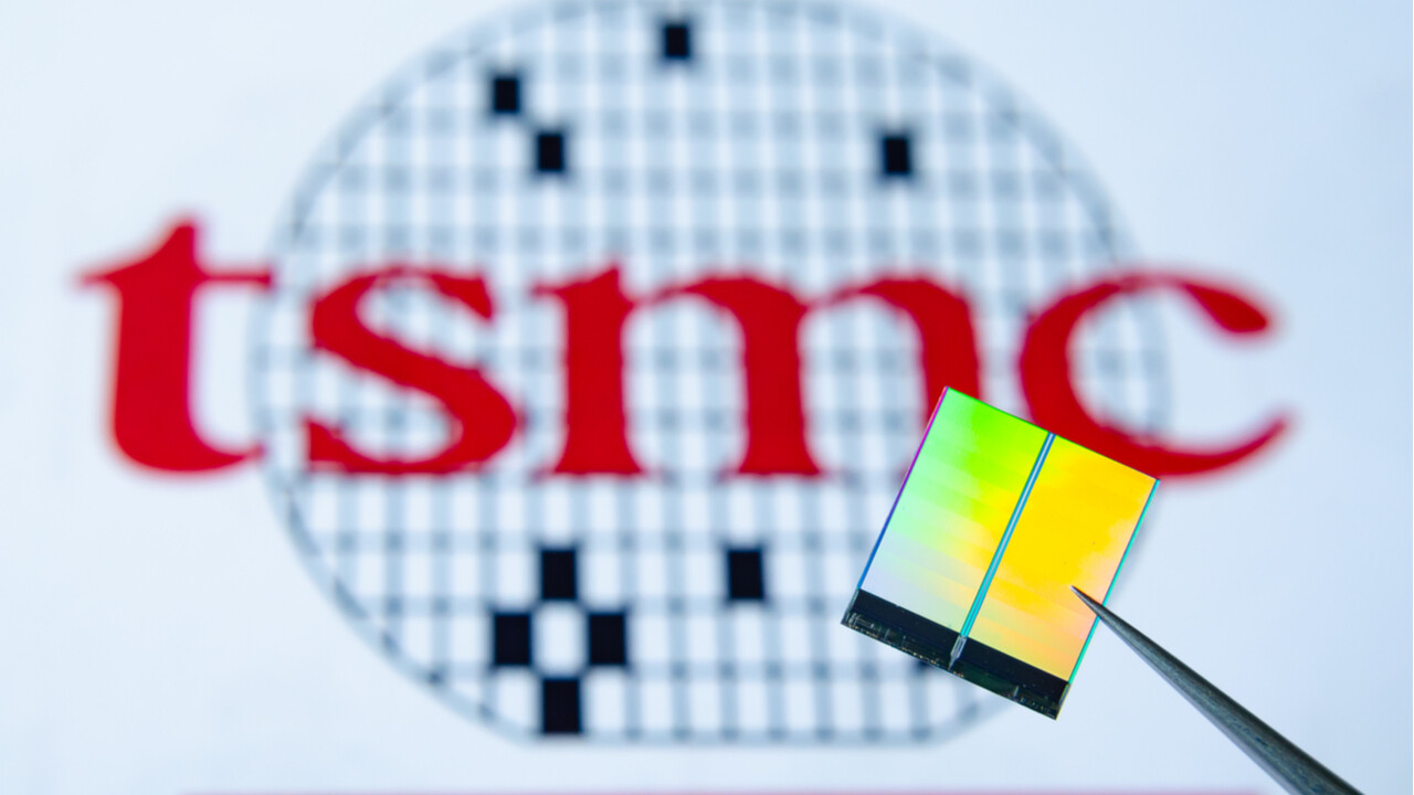
TSMC Claims Breakthrough on 1nm Chip Production
TSMC in collaboration with the National Taiwan University (NTU) and the Massachusetts Institute of Technology (MIT) have made a significant breakthrough in the development of 1-nanometer chips. The joint announcement comes after IBM earlier this month published news of their 2-nanometer chip development. The researchers found that the use of semi-metal bismuth (Bi) as contact electrodes for the 2D matrix can greatly reduce resistance and increase current. This discovery was first made by the MIT team before then being further refined by TSMC and NTU which will increase energy efficiency and performance in future processors. The 1-nanometer node won't be deployed for several years with TSMC planning to start 3-nanometer production in H2 2022.
Source:
Nature
35 Comments on TSMC Claims Breakthrough on 1nm Chip Production
Quantum needs supercooling and until we find a material that will efficiently move heat it will remain in the realm of super computers for large companies and governments.
Honey, can you pick up a gallon of liquid nitrogen, there is a gaming match I need my VR quantum system and it’s going to need it.
I don’t imagine that will become the norm, so classical computing for the near future for us. 3D chips with pathways for phase change heat transfer fluid will be mainstream before quantum chips. Considering that the maximum and actual transistor density is already 2X different to achieve the switching speed required we may even see it happen before “1nm” is in full production. It’s the question of how much is wafer space and product availability worth to add it.
I cannot see at all how they can go into the pico metre range after this, you will have structures that are only a few atoms wide. They actually cease to behave at all like a bulk material. A hydrogen atom is about 1.06Å in diameter and silcon is about 3Å but of course silicon is in a crystal structure and the bond lengths are larger.