Monday, May 29th 2023

TSMC N3 Nodes Show SRAM Scaling is Hitting the Wall
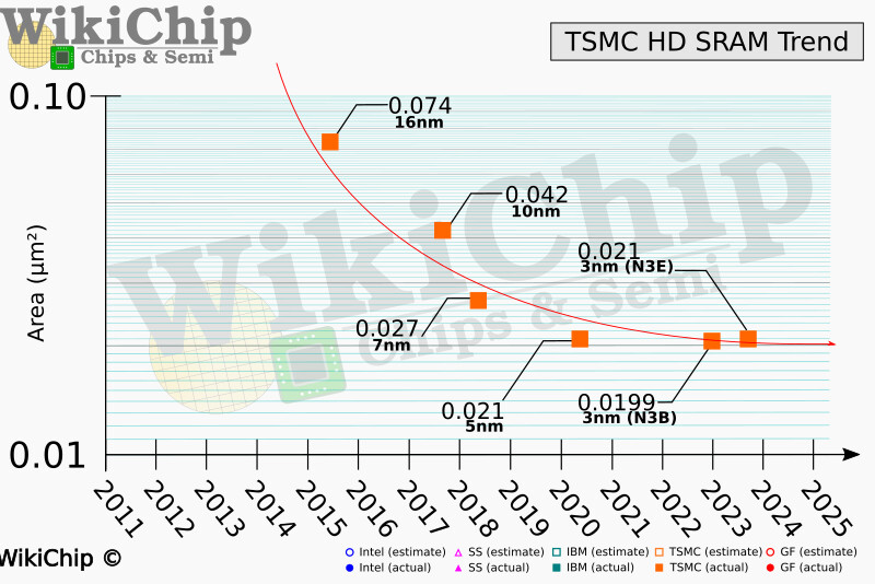
When TSMC introduced its N3 lineup of nodes, the company only talked about the logic scaling of the two new semiconductor manufacturing steps. However, it turns out that there was a reason for it, as WikiChip confirms that the SRAM bit cells of N3 nodes are almost identical to the SRAM bit cells of N5 nodes. At TSMC 2023 Technology Symposium, TSMC presented additional details about its N3 node lineup, including logic and SRAM density. For starters, the N3 node is TSMC's "3 nm" node family that has two products: a Base N3 node (N3B) and an Enhanced N3 node (N3E). The base N3B uses a new (for TSMC) self-aligned contact (SAC) scheme that Intel introduced back in 2011 with a 22 nm node, which improves the node's yield.
Regardless of N3's logic density improvements compared to the "last-generation" N5, the SRAM density is almost identical. Initially, TSMC claimed N3B SRAM density was 1.2x over the N5 process. However, recent information shows that the actual SRAM density is merely a 5% difference. With SRAM taking a large portion of the transistor and area budget of a processor, N3B's soaring manufacturing costs are harder to justify when there is almost no area improvement. For some time, SRAM scaling wasn't following logic scaling; however, the two have now completely decoupled.
Source:
WikiChip
Regardless of N3's logic density improvements compared to the "last-generation" N5, the SRAM density is almost identical. Initially, TSMC claimed N3B SRAM density was 1.2x over the N5 process. However, recent information shows that the actual SRAM density is merely a 5% difference. With SRAM taking a large portion of the transistor and area budget of a processor, N3B's soaring manufacturing costs are harder to justify when there is almost no area improvement. For some time, SRAM scaling wasn't following logic scaling; however, the two have now completely decoupled.
31 Comments on TSMC N3 Nodes Show SRAM Scaling is Hitting the Wall
Yes, optical resolution is a huge hurdle that has been tweaked to the extreme. FinFET was introduced to exchange horizontal space for vertical. GAA takes that another step.Also, L1 in particular, will be multi-ported. These can easily need 10x the real-estate per cell.
*looks at 379m2 geforce 4080*
Yeah I think its a little early to call the chiplet GPU "justified".