Report an Error


AMD Bonaire

Bonaire

Bonaire PRO

Bonaire XT

Bonaire XTX
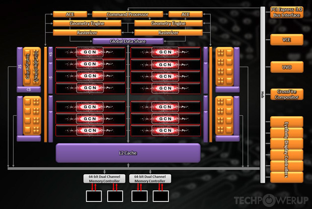
Block Diagram
AMD's Bonaire GPU uses the GCN 2.0 architecture and is made using a 28 nm production process at TSMC. With a die size of 160 mm² and a transistor count of 2,080 million it is a small chip. Bonaire supports DirectX 12 (Feature Level 12_0). For GPU compute applications, OpenCL version 2.1 can be used. It features 896 shading units, 56 texture mapping units and 16 ROPs.
Further reading:
Sea Islands Instruction Set Architecture 
Graphics Processor
- Released
- Mar 22nd, 2013
- GPU Name
- Bonaire
- Desktop Variant
- Tobago
- Mobile Variant
- Saturn / Strato
- Mobile Variant 2
- Emerald
- Generation
- Sea Islands
- Architecture
- GCN 2.0
- Foundry
- TSMC
- Process Size
- 28 nm
- Transistors
- 2,080 million
- Density
- 13.0M / mm²
- Die Size
- 160 mm²
- Package
- FCBGA-1093
Graphics Features
- DirectX
- 12 (12_0)
- OpenGL
- 4.6
- OpenCL
- 2.1
- Vulkan
- 1.2.170
- Shader Model
- 6.5
- WDDM
- 2.7
- Compute
- GFX7 (gfx704)
- DCE
- 8.2
- UVD
- 4.2
- VCE
- 2.0
- SDMA
- 1.0.0
- CLRX
- GCN 1.1.0
Render Config
- Shading Units
- 896
- TMUs
- 56
- ROPs
- 16
- Compute Units
- 14
- Z-Stencil
- 64
- ACEs
- 2
- GEs
- 2
- L1 Cache
- 16 KB per CU
- L2 Cache
- 256 KB
- Max. TDP
- 115 W
All GCN 2.0 GPUs
AMD GPU Architecture History
- 2023 CDNA 3.0
- 2022-2024 RDNA 3.0
- 2021 CDNA 2.0
- 2020 CDNA 1.0
- 2020-2023 RDNA 2.0
- 2019-2020 RDNA 1.0
- 2018-2022 GCN 5.1
- 2017-2020 GCN 5.0
- 2016-2020 GCN 4.0
- 2014-2019 GCN 3.0
- 2013-2017 GCN 2.0
- 2011-2020 GCN 1.0
- 2010-2013 TeraScale 3
- 2009-2015 TeraScale 2
- 2005-2013 TeraScale
- 2005-2007 Ultra-Threaded SE
Graphics cards using the AMD Bonaire GPU
| Name | Chip | Memory | Shaders | TMUs | ROPs | GPU Clock | Memory Clock |
|---|---|---|---|---|---|---|---|
| Bonaire XT | 1024 MB | 896 | 56 | 16 | 1050 MHz | 1500 MHz | |
| Bonaire XT | 1024 MB | 896 | 56 | 16 | 1000 MHz | 1500 MHz | |
| Bonaire XTX | 2 GB | 896 | 56 | 16 | 1100 MHz | 1625 MHz | |
| Bonaire PRO | 2 GB | 768 | 48 | 16 | 1000 MHz | 1500 MHz | |
| Bonaire XTX | 1024 MB | 896 | 56 | 16 | 1100 MHz | 1625 MHz | |
| Bonaire PRO GL | 4 GB | 768 | 48 | 16 | 930 MHz | 1500 MHz | |
| Bonaire PRO GL | 4 GB | 768 | 48 | 16 | 930 MHz | 1500 MHz |


Bonaire GPU Notes
| Generation: Sea Islands Desktop Variant: Tobago Mobile Variant: Saturn / Strato / Emerald Graphics/Compute: GFX7 (gfx704) Display Core Engine: 8.2 Unified Video Decoder: 4.2 Video Compression Engine: 2.0 System DMA: 1.0.0 CLRX: GCN 1.1.0 |
Apr 29th, 2024 17:26 EDT
change timezone
Latest GPU Drivers
New Forum Posts
- EK seems to be having major issues (56)
- 7900 XTX Seriously lacking (11)
- Post your CrystalDiskMark speeds (598)
- i7-1355U (8)
- Is it better for zero RPM PSUs to place the fan on top? (28)
- Looking for recommendations to upgrade the GPU (32)
- What are you playing? (20557)
- Dialing in the overlock on my new 12600kf, matured silicon process showing great results... (33)
- Is this Sapphire PULSE RX 5600 XT legit or fake? (17)
- Show us your collections thread!! (285)
Popular Reviews
- Ugreen NASync DXP4800 Plus Review
- HYTE THICC Q60 240 mm AIO Review
- Upcoming Hardware Launches 2023 (Updated Feb 2024)
- MOONDROP x Crinacle DUSK In-Ear Monitors Review - The Last 5%
- Thermalright Phantom Spirit 120 EVO Review
- AMD Ryzen 7 7800X3D Review - The Best Gaming CPU
- Team Group T-Force Vulcan ECO DDR5-6000 32 GB CL38 Review
- FiiO K19 Desktop DAC/Headphone Amplifier Review
- ASUS Radeon RX 7900 GRE TUF OC Review
- Logitech G Pro X Superlight 2 Review - Updated with 4000 Hz Tested
Controversial News Posts
- Windows 11 Now Officially Adware as Microsoft Embeds Ads in the Start Menu (152)
- Intel Statement on Stability Issues: "Motherboard Makers to Blame" (148)
- Sony PlayStation 5 Pro Specifications Confirmed, Console Arrives Before Holidays (117)
- NVIDIA Points Intel Raptor Lake CPU Users to Get Help from Intel Amid System Instability Issues (106)
- AMD's RDNA 4 GPUs Could Stick with 18 Gbps GDDR6 Memory (103)
- AMD "Strix Halo" Zen 5 Mobile Processor Pictured: Chiplet-based, Uses 256-bit LPDDR5X (103)
- US Government Wants Nuclear Plants to Offload AI Data Center Expansion (98)
- TechPowerUp Hiring: Reviewers Wanted for Motherboards, Laptops, Gaming Handhelds and Prebuilt Desktops (89)