Report an Error


ATI R420
R420

Oleg Kashirin
Die Shot
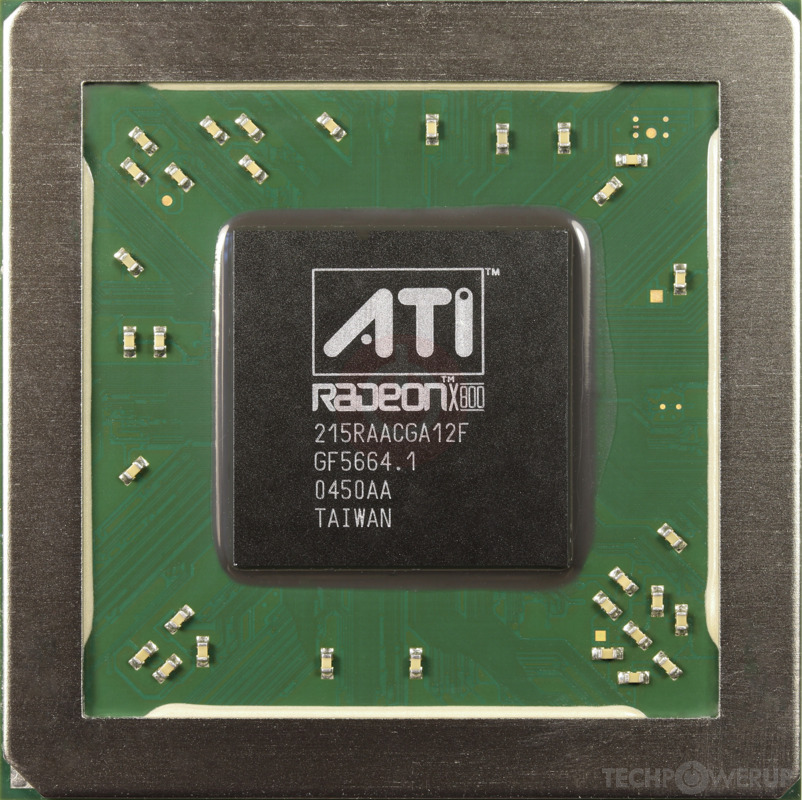
ATI's R420 GPU uses the R400 architecture and is made using a 130 nm production process at TSMC. With a die size of 281 mm² and a transistor count of 160 million it is a medium-sized chip. R420 supports DirectX 9.0b (Feature Level 9_2). Modern GPU compute technologies are not available. It features 16 pixel shaders and 6 vertex shaders, 16 texture mapping units and 16 ROPs. Due to the lack of unified shaders you will not be able to run recent games at all (which require unified shader/DX10+ support).
Graphics Processor
- Released
- Mar 1st, 2004
- GPU Name
- R420
- Mobile Variant
- M18
- Codename
- Loki
- Architecture
- R400
- Foundry
- TSMC
- Process Size
- 130 nm
- Transistors
- 160 million
- Density
- 569.4K / mm²
- Die Size
- 281 mm²
- Package
- FCBGA-1265
- Package Size
- 42.5 mm × 42.5 mm
Graphics Features
- DirectX
- 9.0b (9_2)
- OpenGL
- 2.1
- OpenCL
- N/A
- Vulkan
- N/A
- Pixel Shader
- 2.0b
- Vertex Shader
- 2.0b
- WDDM
- 1.0
- Compute
- GFX2
Render Config
- Pixel Shaders
- 16
- Vertex Shaders
- 6
- TMUs
- 16
- ROPs
- 16
- Max. TDP
- 63 W
All R400 GPUs
ATI GPU Architecture History
Graphics cards using the ATI R420 GPU
| Name | Chip | Memory | Shaders | TMUs | ROPs | GPU Clock | Memory Clock |
|---|---|---|---|---|---|---|---|
| R420 XTP | 256 MB | 16 / 6 | 16 | 16 | 520 MHz | 560 MHz | |
| R420 PRO | 256 MB | 12 / 6 | 12 | 12 | 475 MHz | 450 MHz | |
| R420 XT | 256 MB | 16 / 6 | 16 | 16 | 500 MHz | 500 MHz | |
| R420 LE | 256 MB | 8 / 6 | 8 | 8 | 450 MHz | 400 MHz | |
| R420 XT | 256 MB | 16 / 6 | 16 | 16 | 500 MHz | 500 MHz | |
| R420 GL | 256 MB | 12 / 6 | 12 | 12 | 491 MHz | 454 MHz | |
| R420 LE | 256 MB | 8 / 6 | 8 | 8 | 425 MHz | 400 MHz | |
| R420 PRO | 256 MB | 12 / 6 | 12 | 12 | 400 MHz | 490 MHz | |
| R420 LE | 256 MB | 8 / 6 | 8 | 8 | 473 MHz | 493 MHz | |
| R420 XT | 256 MB | 16 / 6 | 16 | 16 | 425 MHz | 398 MHz | |
| R420 LE | 256 MB | 8 / 6 | 8 | 8 | 425 MHz | 400 MHz |


R420 GPU Notes
| Mobile Variant: M18 Codename: Loki Graphics/Compute: GFX2 Smart Shader HD Smooth Vision HD TruForm 2.0 Hyper Z HD Video Shader HD 3Dc Compression Programmable pixel&vertex pipelines |
May 3rd, 2024 20:10 EDT
change timezone
Latest GPU Drivers
New Forum Posts
- Change GPU or PSU ? Games look cryspy and sharp with microsuttering (0)
- Should I install Windows 10 or 11 for my new device (63)
- AM5 Motherboard Question, which of these two should I go with? (10)
- Ryzen 7800x3d $196 with bundle at Microcenter (26)
- 7800x3d $216 in bundle at Microcenter (38)
- AMD Radeon Pro v540 Research Thread (251)
- Need advice for UPS that will be use only for bios updates (7)
- Keysfan (9)
- Announcement: VPN's no longer work right in Windows 10 or 11 or Servers (31)
- Which PSU to take? (54)
Popular Reviews
- ASRock NUC BOX-155H (Intel Core Ultra 7 155H) Review
- Meze Audio LIRIC 2nd Generation Closed-Back Headphones Review
- Finalmouse UltralightX Review
- Montech Sky Two GX Review
- Gigabyte GeForce RTX 4070 Ti Super Gaming OC Review
- Upcoming Hardware Launches 2023 (Updated Feb 2024)
- HYTE THICC Q60 240 mm AIO Review
- Alienware Pro Wireless Gaming Keyboard Review
- Ugreen NASync DXP4800 Plus Review
- Team Group T-Force Vulcan ECO DDR5-6000 32 GB CL38 Review
Controversial News Posts
- Intel Statement on Stability Issues: "Motherboard Makers to Blame" (235)
- Windows 11 Now Officially Adware as Microsoft Embeds Ads in the Start Menu (167)
- Sony PlayStation 5 Pro Specifications Confirmed, Console Arrives Before Holidays (117)
- AMD's RDNA 4 GPUs Could Stick with 18 Gbps GDDR6 Memory (114)
- AMD to Redesign Ray Tracing Hardware on RDNA 4 (113)
- NVIDIA Points Intel Raptor Lake CPU Users to Get Help from Intel Amid System Instability Issues (106)
- AMD "Strix Halo" Zen 5 Mobile Processor Pictured: Chiplet-based, Uses 256-bit LPDDR5X (103)
- AMD Ryzen 9 7900X3D Now at a Mouth-watering $329 (103)