Report an Error


NVIDIA GP107S

GP107S

GP107-670-A1

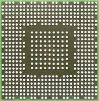
GP107S BGA

Block Diagram
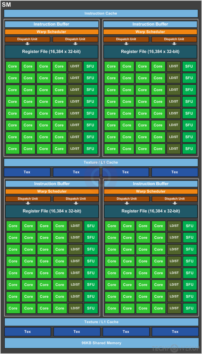
SM Diagram
NVIDIA's GP107S GPU uses the Pascal architecture and is made using a 14 nm production process at Samsung. With a die size of 132 mm² and a transistor count of 3,300 million it is a small chip. GP107S supports DirectX 12 (Feature Level 12_1). For GPU compute applications, OpenCL version 3.0 and CUDA 6.1 can be used. It features 640 shading units, 32 texture mapping units and 16 ROPs.
Graphics Processor
- Released
- Feb 10th, 2020
- GPU Name
- GP107S
- Codename
- NV137
- Architecture
- Pascal
- Foundry
- Samsung
- Process Size
- 14 nm
- Transistors
- 3,300 million
- Density
- 25.0M / mm²
- Die Size
- 132 mm²
- Package
- BGA-595
Graphics Features
- DirectX
- 12 (12_1)
- OpenGL
- 4.6
- OpenCL
- 3.0
- Vulkan
- 1.3
- CUDA
- 6.1
- Shader Model
- 6.7
- WDDM
- 3.1
- NVENC
- No Support
- NVDEC
- 3rd Gen
- PureVideo HD
- VP8
- VDPAU
- Feature Set H
Render Config
- Shading Units
- 640
- TMUs
- 32
- ROPs
- 16
- SM Count
- 5
- SFUs
- 192
- TPCs
- 6
- GPCs
- 2
- L1 Cache
- 48 KB per SM
- L2 Cache
- 512 KB
- Max. TDP
- 20 W
All Pascal GPUs
NVIDIA GPU Architecture History
- 2024 Blackwell
- 2023 Hopper
- 2022-2024 Ada Lovelace
- 2020-2024 Ampere
- 2018-2022 Turing
- 2017-2020 Volta
- 2016-2021 Pascal
- 2014-2019 Maxwell 2.0
- 2014-2017 Maxwell
- 2013-2015 Kepler 2.0
- 2012-2018 Kepler
- 2010-2016 Fermi 2.0
- 2010-2013 VLIW Vec4
- 2010-2016 Fermi
- 2007-2013 Tesla 2.0
- 2006-2010 Tesla
- 2003-2013 Curie
- 2003-2005 Rankine
- 2001-2003 Kelvin
- 1999-2005 Celsius
- 1998-2000 Fahrenheit
Graphics cards using the NVIDIA GP107S GPU
| Name | Chip | Memory | Shaders | TMUs | ROPs | Base Clock | Boost Clock | Memory Clock |
|---|---|---|---|---|---|---|---|---|
| GP107-670-A1 | 2 GB | 640 | 32 | 16 | 1354 MHz | 1468 MHz | 1752 MHz | |
| GP107-670-A1 | 2 GB | 640 | 32 | 16 | 747 MHz | 937 MHz | 1752 MHz |
GP107S GPU Notes
| NVENC: No Support NVDEC: 3rd Gen PureVideo HD: VP8 VDPAU: Feature Set H |
May 16th, 2024 16:51 EDT
change timezone
Latest GPU Drivers
New Forum Posts
- Struck out with Asus X670E-F board, continuous 10500Hz squeal, recommend my next gamble (15)
- Dell Workstation Owners Club (3088)
- EK seems to be having major issues (79)
- 20 Years? (33)
- NVcleanstall error (7)
- Homeworld 3 [Official Thread] (45)
- Failed to use desktop vga with laptop. (eGPU) (39)
- AM5 boot times improve RADICALLY with memory context restore enabled (73)
- Virtual desktops and Chrome browser (6)
- Unknown Subvendor in GPU-Z (3)
Popular Reviews
- Homeworld 3 Performance Benchmark Review - 35 GPUs Tested
- Enermax REVOLUTION D.F. X 1200 W Review
- Lofree Edge Ultra-Low Profile Wireless Mechanical Keyboard Review
- Silverstone Shark Force 120 mm Fan Review
- Upcoming Hardware Launches 2023 (Updated Feb 2024)
- ZMF Caldera Closed Planar Magnetic Headphones Review
- AMD Ryzen 7 7800X3D Review - The Best Gaming CPU
- Corsair MP700 Pro SE 4 TB Review
- ASUS Radeon RX 7900 GRE TUF OC Review
- Sapphire Radeon RX 7900 GRE Pulse Review
Controversial News Posts
- Intel Statement on Stability Issues: "Motherboard Makers to Blame" (267)
- AMD to Redesign Ray Tracing Hardware on RDNA 4 (227)
- Windows 11 Now Officially Adware as Microsoft Embeds Ads in the Start Menu (172)
- NVIDIA to Only Launch the Flagship GeForce RTX 5090 in 2024, Rest of the Series in 2025 (152)
- AMD Hits Highest-Ever x86 CPU Market Share in Q1 2024 Across Desktop and Server (137)
- AMD RDNA 5 a "Clean Sheet" Graphics Architecture, RDNA 4 Merely Corrects a Bug Over RDNA 3 (128)
- AMD's RDNA 4 GPUs Could Stick with 18 Gbps GDDR6 Memory (114)
- AMD Ryzen 9 7900X3D Now at a Mouth-watering $329 (104)