Report an Error


NVIDIA TU116B
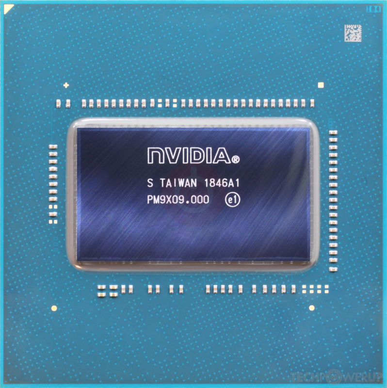
TU116B

Die Shot

Block Diagram

SM Diagram
NVIDIA's TU116B GPU uses the Turing architecture and is made using a 12 nm production process at TSMC. With a die size of 284 mm² and a transistor count of 6,600 million it is a medium-sized chip. TU116B supports DirectX 12 (Feature Level 12_1). For GPU compute applications, OpenCL version 3.0 and CUDA 7.5 can be used. It features 1536 shading units, 96 texture mapping units and Unknown ROPs.
Further reading:
Turing Architecture Whitepaper 
Graphics Processor
- Released
- Unknown
- GPU Name
- TU116B
- Codename
- NV168
- Architecture
- Turing
- Foundry
- TSMC
- Process Type
- 12FFN FinFET
- Process Size
- 12 nm
- Transistors
- 6,600 million
- Density
- 23.2M / mm²
- Die Size
- 284 mm²
- Package
- BGA-2228
- Package Size
- 37.5 mm × 37.5 mm
Graphics Features
- DirectX
- 12 (12_1)
- OpenGL
- 4.6
- OpenCL
- 3.0
- Vulkan
- 1.3
- CUDA
- 7.5
- Shader Model
- 6.7
- WDDM
- 3.1
- NVENC
- 7th Gen
- NVDEC
- 4th Gen
- PureVideo HD
- VP10
- VDPAU
- Feature Set J
Render Config
- Shading Units
- 1536
- TMUs
- 96
- ROPs
- Unknown
- SM Count
- 24
- FP16 Units
- 3072
- FP64 Units
- 48
- SFUs
- 384
- TPCs
- 12
- GPCs
- 3
- Tex L1 Cache
- 32 KB per SM
All Turing GPUs
NVIDIA GPU Architecture History
- 2024 Blackwell
- 2023 Hopper
- 2022-2024 Ada Lovelace
- 2020-2024 Ampere
- 2018-2022 Turing
- 2017-2020 Volta
- 2016-2021 Pascal
- 2014-2019 Maxwell 2.0
- 2014-2017 Maxwell
- 2013-2015 Kepler 2.0
- 2012-2018 Kepler
- 2010-2016 Fermi 2.0
- 2010-2013 VLIW Vec4
- 2010-2016 Fermi
- 2007-2013 Tesla 2.0
- 2006-2010 Tesla
- 2003-2013 Curie
- 2003-2005 Rankine
- 2001-2003 Kelvin
- 1999-2005 Celsius
- 1998-2000 Fahrenheit
TU116B GPU Notes
| NVENC: 7th Gen NVDEC: 4th Gen PureVideo HD: VP10 VDPAU: Feature Set J |
May 15th, 2024 23:41 EDT
change timezone
Latest GPU Drivers
New Forum Posts
- LOL ASUS says this is $200 in repair, Steve from gamers Nexus smokes ASUS, Steam Deck til I die boys!!!! (81)
- RMAd every single component in my PC, and it's still crashing (15)
- Ryzen Owners Zen Garden (7363)
- Last game you purchased? (296)
- RTX 4090 VS Titan Volta or titan RTX (7)
- MSI Z370 SLI PLUS + i9 9900k bad perfomance. (0)
- 20 Years? (14)
- I just succesfully baked DDR4 (96)
- Homeworld 3 [Official Thread] (41)
- Air makes its way from the reservoir into the radiator. (79)
Popular Reviews
- Homeworld 3 Performance Benchmark Review - 35 GPUs Tested
- Enermax REVOLUTION D.F. X 1200 W Review
- Upcoming Hardware Launches 2023 (Updated Feb 2024)
- Lofree Edge Ultra-Low Profile Wireless Mechanical Keyboard Review
- ZMF Caldera Closed Planar Magnetic Headphones Review
- AMD Ryzen 7 7800X3D Review - The Best Gaming CPU
- Corsair MP700 Pro SE 4 TB Review
- ASUS Radeon RX 7900 GRE TUF OC Review
- ThundeRobot ML903 NearLink Review
- Sapphire Radeon RX 7900 GRE Pulse Review
Controversial News Posts
- Intel Statement on Stability Issues: "Motherboard Makers to Blame" (267)
- AMD to Redesign Ray Tracing Hardware on RDNA 4 (227)
- Windows 11 Now Officially Adware as Microsoft Embeds Ads in the Start Menu (172)
- NVIDIA to Only Launch the Flagship GeForce RTX 5090 in 2024, Rest of the Series in 2025 (152)
- AMD Hits Highest-Ever x86 CPU Market Share in Q1 2024 Across Desktop and Server (137)
- AMD RDNA 5 a "Clean Sheet" Graphics Architecture, RDNA 4 Merely Corrects a Bug Over RDNA 3 (124)
- AMD's RDNA 4 GPUs Could Stick with 18 Gbps GDDR6 Memory (114)
- AMD Ryzen 9 7900X3D Now at a Mouth-watering $329 (104)