Report an Error


NVIDIA T500 Mobile
- Graphics Processor
- TU117
- Cores
- 896
- TMUs
- 56
- ROPs
- 32
- Memory Size
- 4 GB
- Memory Type
- GDDR6
- Bus Width
- 64 bit
GPU
Recommended Gaming Resolutions:
- 1920x1080
- 2560x1440
- 3840x2160
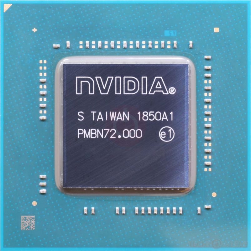
The T500 Mobile is a professional mobile graphics chip by NVIDIA, launched on December 2nd, 2020. Built on the 12 nm process, and based on the TU117 graphics processor, the chip supports DirectX 12. The TU117 graphics processor is an average sized chip with a die area of 200 mm² and 4,700 million transistors. It features 896 shading units, 56 texture mapping units, and 32 ROPs. NVIDIA has paired 4 GB GDDR6 memory with the T500 Mobile, which are connected using a 64-bit memory interface. The GPU is operating at a frequency of 1185 MHz, which can be boosted up to 1560 MHz, memory is running at 1250 MHz (10 Gbps effective).
Its power draw is rated at 18 W maximum. This device has no display connectivity, as it is not designed to have monitors connected to it. Rather it is intended for use in laptop/notebooks and will use the output of the host mobile device. T500 Mobile is connected to the rest of the system using a PCI-Express 3.0 x16 interface.
Its power draw is rated at 18 W maximum. This device has no display connectivity, as it is not designed to have monitors connected to it. Rather it is intended for use in laptop/notebooks and will use the output of the host mobile device. T500 Mobile is connected to the rest of the system using a PCI-Express 3.0 x16 interface.
Graphics Processor
Mobile Graphics
- Release Date
- Dec 2nd, 2020
- Generation
-
Quadro Turing-M
(Tx000)
- Predecessor
- Quadro Pascal-M
- Successor
- Quadro Ampere-M
- Production
- Active
- Bus Interface
- PCIe 3.0 x16
Relative Performance
Based on TPU review data: "Performance Summary" at 1920x1080, 4K for 2080 Ti and faster.
Performance estimated based on architecture, shader count and clocks.
Clock Speeds
- Base Clock
- 1185 MHz
- Boost Clock
- 1560 MHz
- Memory Clock
-
1250 MHz
10 Gbps effective
Memory
- Memory Size
- 4 GB
- Memory Type
- GDDR6
- Memory Bus
- 64 bit
- Bandwidth
- 80.00 GB/s
Render Config
- Shading Units
- 896
- TMUs
- 56
- ROPs
- 32
- SM Count
- 14
- L1 Cache
- 64 KB (per SM)
- L2 Cache
- 1024 KB
Theoretical Performance
- Pixel Rate
- 49.92 GPixel/s
- Texture Rate
- 87.36 GTexel/s
- FP16 (half)
- 5.591 TFLOPS (2:1)
- FP32 (float)
- 2.796 TFLOPS
- FP64 (double)
- 87.36 GFLOPS (1:32)
Board Design
- Slot Width
- IGP
- TDP
- 18 W
- Outputs
- Portable Device Dependent
- Power Connectors
- None
- Board Number
- E3903 SKU 10
Graphics Features
- DirectX
- 12 (12_1)
- OpenGL
- 4.6
- OpenCL
- 3.0
- Vulkan
- 1.3
- CUDA
- 7.5
- Shader Model
- 6.7
TU117 GPU Notes
| NVENC: 5th Gen NVDEC: 4th Gen PureVideo HD: VP10 VDPAU: Feature Set J |
Devices based on this design (5)
| Name | GPU Clock | Boost Clock | Memory Clock | Other Changes |
|---|---|---|---|---|
| 1365 MHz | 1695 MHz | 1250 MHz | 2 GB, 25 W | |
| 1365 MHz | 1695 MHz | 1250 MHz | 25 W | |
| 1185 MHz | 1560 MHz | 1250 MHz | ||
| 1365 MHz | 1695 MHz | 1250 MHz | 25 W | |
| 1365 MHz | 1695 MHz | 1250 MHz | 25 W |
May 16th, 2024 04:35 EDT
change timezone
Latest GPU Drivers
New Forum Posts
- Immortals of Aveum deserves a second chance, the new free demo has convinced me. (48)
- EULA in Games (10)
- Double radiator setup with GPU fans on top (5)
- What's your latest tech purchase? (20532)
- Apparently Valve is giving refunds on Helldivers 2 regardless of hour count. Details inside. (108)
- AM5 boot times improve RADICALLY with memory context restore enabled (69)
- MSI Z370 SLI PLUS + i9 9900k bad perfomance. (3)
- have LGA 1155 motherboard which xeon processor will fit ? (15)
- Ubuntu 24.04 LTS released (29)
- NVcleanstall error (3)
Popular Reviews
- Homeworld 3 Performance Benchmark Review - 35 GPUs Tested
- Enermax REVOLUTION D.F. X 1200 W Review
- Lofree Edge Ultra-Low Profile Wireless Mechanical Keyboard Review
- Upcoming Hardware Launches 2023 (Updated Feb 2024)
- ZMF Caldera Closed Planar Magnetic Headphones Review
- AMD Ryzen 7 7800X3D Review - The Best Gaming CPU
- Corsair MP700 Pro SE 4 TB Review
- ASUS Radeon RX 7900 GRE TUF OC Review
- ThundeRobot ML903 NearLink Review
- Sapphire Radeon RX 7900 GRE Pulse Review
Controversial News Posts
- Intel Statement on Stability Issues: "Motherboard Makers to Blame" (267)
- AMD to Redesign Ray Tracing Hardware on RDNA 4 (227)
- Windows 11 Now Officially Adware as Microsoft Embeds Ads in the Start Menu (172)
- NVIDIA to Only Launch the Flagship GeForce RTX 5090 in 2024, Rest of the Series in 2025 (152)
- AMD Hits Highest-Ever x86 CPU Market Share in Q1 2024 Across Desktop and Server (137)
- AMD RDNA 5 a "Clean Sheet" Graphics Architecture, RDNA 4 Merely Corrects a Bug Over RDNA 3 (124)
- AMD's RDNA 4 GPUs Could Stick with 18 Gbps GDDR6 Memory (114)
- AMD Ryzen 9 7900X3D Now at a Mouth-watering $329 (104)