News Posts matching #AI

Return to Keyword Browsing

Groq LPU AI Inference Chip is Rivaling Major Players like NVIDIA, AMD, and Intel

AI workloads are split into two different categories: training and inference. While training requires large computing and memory capacity, access speeds are not a significant contributor; inference is another story. With inference, the AI model must run extremely fast to serve the end-user with as many tokens (words) as possible, hence giving the user answers to their prompts faster. An AI chip startup, Groq, which was in stealth mode for a long time, has been making major moves in providing ultra-fast inference speeds using its Language Processing Unit (LPU) designed for large language models (LLMs) like GPT, Llama, and Mistral LLMs. The Groq LPU is a single-core unit based on the Tensor-Streaming Processor (TSP) architecture which achieves 750 TOPS at INT8 and 188 TeraFLOPS at FP16, with 320x320 fused dot product matrix multiplication, in addition to 5,120 Vector ALUs.

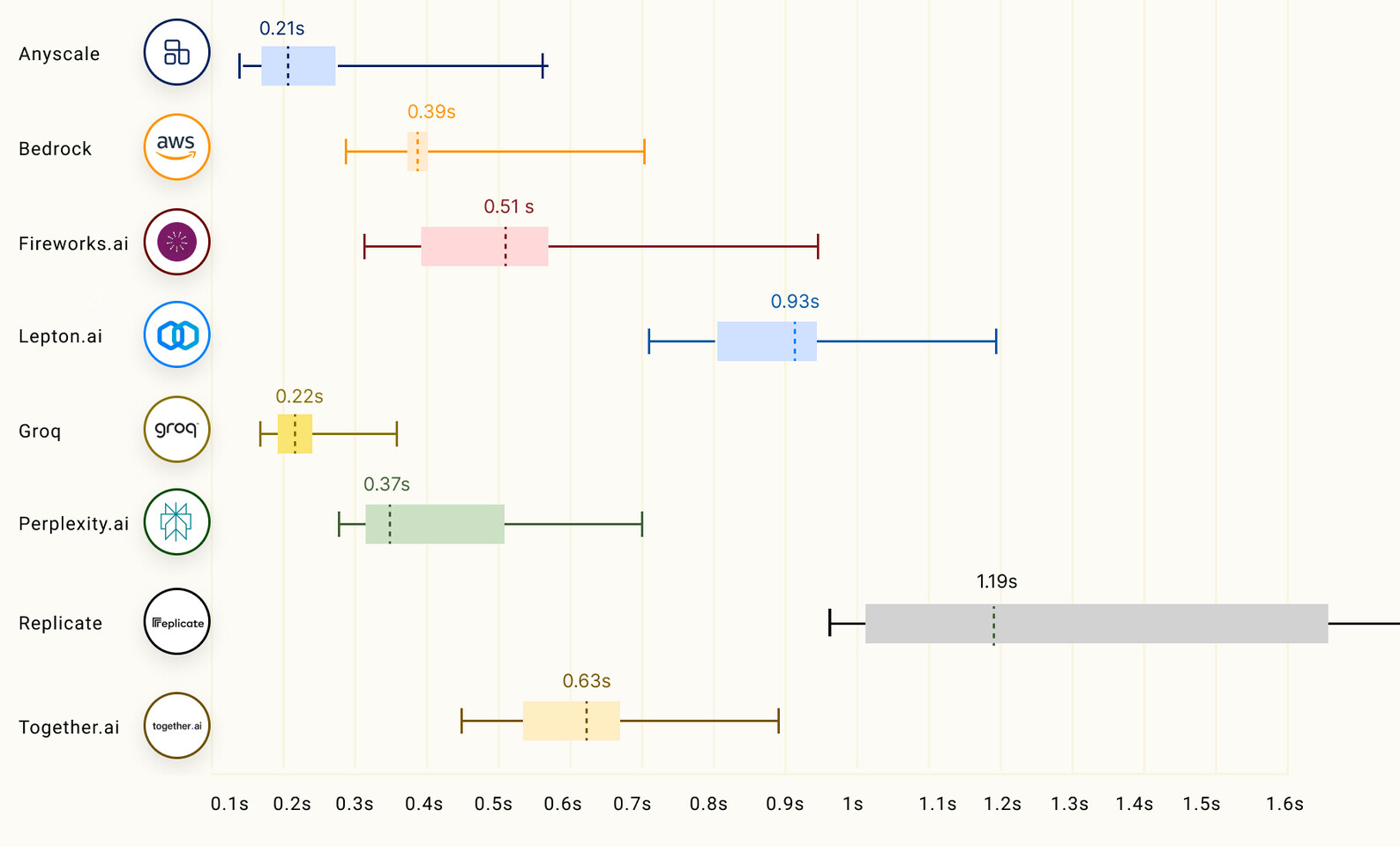
Having massive concurrency with 80 TB/s of bandwidth, the Groq LPU has 230 MB capacity of local SRAM. All of this is working together to provide Groq with a fantastic performance, making waves over the past few days on the internet. Serving the Mixtral 8x7B model at 480 tokens per second, the Groq LPU is providing one of the leading inference numbers in the industry. In models like Llama 2 70B with 4096 token context length, Groq can serve 300 tokens/s, while in smaller Llama 2 7B with 2048 tokens of context, Groq LPU can output 750 tokens/s. According to the LLMPerf Leaderboard, the Groq LPU is beating the GPU-based cloud providers at inferencing LLMs Llama in configurations of anywhere from 7 to 70 billion parameters. In token throughput (output) and time to first token (latency), Groq is leading the pack, achieving the highest throughput and second lowest latency.

GlobalFoundries and Biden-Harris Administration Announce CHIPS and Science Act Funding for Essential Chip Manufacturing

The U.S. Department of Commerce today announced $1.5 billion in planned direct funding for GlobalFoundries (Nasdaq: GFS) (GF) as part of the U.S. CHIPS and Science Act. This investment will enable GF to expand and create new manufacturing capacity and capabilities to securely produce more essential chips for automotive, IoT, aerospace, defense, and other vital markets.

New York-headquartered GF, celebrating its 15th year of operations, is the only U.S.-based pure play foundry with a global manufacturing footprint including facilities in the U.S., Europe, and Singapore. GF is the first semiconductor pure play foundry to receive a major award (over $1.5 billion) from the CHIPS and Science Act, designed to strengthen American semiconductor manufacturing, supply chains and national security. The proposed funding will support three GF projects:

NVIDIA Joins US Artificial Intelligence Safety Institute Consortium

NVIDIA has joined the National Institute of Standards and Technology's new U.S. Artificial Intelligence Safety Institute Consortium as part of the company's effort to advance safe, secure and trustworthy AI. AISIC will work to create tools, methodologies and standards to promote the safe and trustworthy development and deployment of AI. As a member, NVIDIA will work with NIST—an agency of the U.S. Department of Commerce—and fellow consortium members to advance the consortium's mandate. NVIDIA's participation builds on a record of working with governments, researchers and industries of all sizes to help ensure AI is developed and deployed safely and responsibly.

Through a broad range of development initiatives, including NeMo Guardrails, open-source software for ensuring large language model responses are accurate, appropriate, on topic and secure, NVIDIA actively works to make AI safety a reality. In 2023, NVIDIA endorsed the Biden Administration's voluntary AI safety commitments. Last month, the company announced a $30 million contribution to the U.S. National Science Foundation's National Artificial Intelligence Research Resource pilot program, which aims to broaden access to the tools needed to power responsible AI discovery and innovation.

Cervoz Embraces Edge Computing with its M.2 Compact Solutions

Seizing the Edge: Cervoz Adapts to Shifting Data Landscape—The rapid emergence of technologies like AIoT and 5G and their demand for high-speed data processing has accelerated the data transition from the cloud to the edge. This shift exposes data to unpredictable environments with extreme temperature variations, vibrations, and space constraints, making it critical for edge devices to thrive in these settings. Cervoz strategically targets the blooming edge computing sector by introducing an extensive array of compact product lines, enhancing its existing SSDs, DRAM, and Modular Expansion Cards to meet the unique needs of edge computing.

Cervoz Reveals NVMe M.2 SSDs and Connectivity Solutions to Power the Edge
Cervoz introduces its latest compact PCIe Gen. 3x2 SSD offerings, the T421 M.2 2242 (B+M key) and T425 M.2 2230 (A+E key). These space-efficient design and low power consumption feature offer exceptional performance, catering to the storage needs of fanless embedded PCs and motherboards for purpose-built edge applications. Cervoz is also leading the way in developing connectivity solutions, including Ethernet, Wi-Fi, Serial, USB, and CAN Bus all available in M.2 2230 (A+E key) and M.2 2242/2260/2280 (B+M) form factors. The M.2 (B+M key) 2242/2260/2280 card is a versatile three-in-one solution designed for maximum adaptability. While it initially comes in a 2280 form factor, it can be easily adjusted to fit 2260 or 2242 sizes. It offers an effortless upgrade of existing systems without sacrificing connection capability, especially in edge devices.

Samsung & Vodafone "Open RAN Ecosystem" Bolstered by AMD EPYC 8004 Series

Samsung Electronics and Vodafone, in collaboration with AMD, today announced that the three companies have successfully demonstrated an end-to-end call with the latest AMD processors enabling Open RAN technology, a first for the industry. This joint achievement represents the companies' technical leadership in enriching the Open RAN ecosystem throughout the industry. Conducted in Samsung's R&D lab in Korea, the first call was completed using Samsung's versatile, O-RAN-compliant, virtualized RAN (vRAN) software, powered by AMD EPYC 8004 Series processors on Supermicro's Telco/Edge servers, supported by Wind River Studio Container-as-a-Service (CaaS) platform. This demonstration aimed to verify optimized performance, energy efficiency and interoperability among partners' solutions.

The joint demonstration represents Samsung and Vodafone's ongoing commitment to reinforce their position in the Open RAN market and expand their ecosystem with industry-leading partners. This broader and growing Open RAN ecosystem helps operators to build and modernize mobile networks with greater flexibility, faster time-to-market (TTM), and unmatched performance. "Open RAN represents the forthcoming major transformation in advancing mobile networks for the future. Reaching this milestone with top industry partners like Samsung and AMD shows Vodafone's dedication to delivering on the promise of Open RAN innovation," said Nadia Benabdallah, Network Strategy and Engineering Director at Vodafone Group. "Vodafone is continually looking to innovate its network by exploring the potential and diversity of the ecosystem."

GIGABYTE Elevates Computing Horizons at SupercomputingAsia 2024

GIGABYTE, a global leader in high-performance computing solutions, collaborates with industry partner Xenon at SupercomputingAsia 2024, held at the Sydney International Convention and Exhibition Centre from February 19 to 22. This collaboration showcases cutting-edge technologies, offering diverse solutions that redefine the high-performance computing landscape.

GIGABYTE's Highlights at SCA 2024
At booth 19, GIGABYTE presents the G593-SD0, our flagship AI server, and the industry's first Nvidia-certified HGX H100 8-GPU Server. Equipped with 4th/5th Gen Intel Xeon Scalable Processors, it incorporates GIGABYTE's thermal design, ensuring optimal performance within its density-optimized 5U server chassis, pushing the boundaries of AI computing. Additionally, GIGABYTE introduces the 2U 4-node H263-S62 server, designed for 4th Gen Intel Xeon Scalable Processors and now upgraded to the latest 5th Gen, tailored for hybrid and private cloud applications. It features a DLC (Direct Liquid Cooling) solution to efficiently manage heat generated by high-performance computing. Also on display is the newly released W773-W80 workstation, supporting the latest NVIDIA RTX 6000 Ada and catering to CAD, DME, research, data and image analysis, and SMB private cloud applications. At SCA 2024, explore our offerings, including rackmount servers and motherboards, reflecting GIGABYTE's commitment to innovative and reliable solutions. This offers a valuable opportunity to discuss your IT infrastructure requirements with our sales and consulting teams, supported by GIGABYTE and Xenon in Australia.

SoftBank Founder Wants $100 Billion to Compete with NVIDIA's AI

Japanese tech billionaire and founder of the SoftBank Group, Masayoshi Son, is embarking on a hugely ambitious new project to build an AI chip company that aims to rival NVIDIA, the current leader in AI semiconductor solutions. Codenamed "Izanagi" after the Japanese god of creation, Son aims to raise up to $100 billion in funding for the new venture. With his company SoftBank having recently scaled back investments in startups, Son is now setting his sights on the red-hot AI chip sector. Izanagi would leverage SoftBank's existing chip design firm, Arm, to develop advanced semiconductors tailored for artificial intelligence computing. The startup would use Arm's instruction set for the chip's processing elements. This could pit Izanagi directly against NVIDIA's leadership position in AI chips. Son has a chest of $41 billion in cash at SoftBank that he can deploy for Izanagi.

Additionally, he is courting sovereign wealth funds in the Middle East to contribute up to $70 billion in additional capital. In total, Son may be seeking up to $100 billion to bankroll Izanagi into a chip powerhouse. AI chips are seeing surging demand as machine learning and neural networks require specialized semiconductors that can process massive datasets. NVIDIA and other names like Intel, AMD, and select startups have capitalized on this trend. However, Son believes the market has room for another major player. Izanagi would focus squarely on developing bleeding-edge AI chip architectures to power the next generation of artificial intelligence applications. It is still unclear if this would be an AI training or AI inference project, but given that the training market is currently bigger as we are in the early buildout phase of AI infrastructure, the consensus might settle on training. With his track record of bold bets, Son is aiming very high with Izanagi. It's a hugely ambitious goal, but Son has defied expectations before. Project Izanagi will test the limits of even his vision and financial firepower.

Jim Keller Offers to Design AI Chips for Sam Altman for Less Than $1 Trillion

In case you missed it, Sam Altman of OpenAI took the Internet by storm late last week with the unveiling of Sora, the generative AI that can congure up photoreal video clips based on prompts, with deadly accuracy. While Altman and his colleagues in the generative AI industry had a ton of fun generating videos based on prompts from the public on X; it became all too clear that the only thing holding back the democratization of generative AI is the volume of AI accelerator chips. Altman wants to solve this by designing his own AI acceleration hardware from the grounds up, for which he initially pitched an otherworldly $7 trillion in investment—something impossible with the financial markets, but one that's possible only by "printing money," or through sovereign wealth fund investments.

Jim Keller needs no introduction—the celebrity VLSI architect has been designing number crunching devices of all shapes and sizes for some of the biggest tech companies out there for decades, including Intel, Apple, and AMD, just to name a few. When as part of his "are you not entertained?" victory lap, Altman suggested that his vision for the future needs an even larger $8 trillion investment, Keller responded that he could design an AI chip for less than $1 trillion. Does Altman really need several trillions of Dollars to build a grounds-up AI chip at the costs and volumes needed to mainstream AI?

NVIDIA Unveils "Eos" to Public - a Top Ten Supercomputer

Providing a peek at the architecture powering advanced AI factories, NVIDIA released a video that offers the first public look at Eos, its latest data-center-scale supercomputer. An extremely large-scale NVIDIA DGX SuperPOD, Eos is where NVIDIA developers create their AI breakthroughs using accelerated computing infrastructure and fully optimized software. Eos is built with 576 NVIDIA DGX H100 systems, NVIDIA Quantum-2 InfiniBand networking and software, providing a total of 18.4 exaflops of FP8 AI performance. Revealed in November at the Supercomputing 2023 trade show, Eos—named for the Greek goddess said to open the gates of dawn each day—reflects NVIDIA's commitment to advancing AI technology.

Eos Supercomputer Fuels Innovation
Each DGX H100 system is equipped with eight NVIDIA H100 Tensor Core GPUs. Eos features a total of 4,608 H100 GPUs. As a result, Eos can handle the largest AI workloads to train large language models, recommender systems, quantum simulations and more. It's a showcase of what NVIDIA's technologies can do, when working at scale. Eos is arriving at the perfect time. People are changing the world with generative AI, from drug discovery to chatbots to autonomous machines and beyond. To achieve these breakthroughs, they need more than AI expertise and development skills. They need an AI factory—a purpose-built AI engine that's always available and can help ramp their capacity to build AI models at scale Eos delivers. Ranked No. 9 in the TOP 500 list of the world's fastest supercomputers, Eos pushes the boundaries of AI technology and infrastructure.

Intel to Present "AI Everywhere" Innovations at MWC Barcelona 2024

At MWC Barcelona 2024, Intel will demonstrate breakthrough innovations across a full spectrum of new hardware, software and services—bringing AI Everywhere - for the network, edge and enterprise in collaboration with the support and enablement of more than 65 pioneering customers and partners. Announcements will span AI network innovations, edge AI platforms, Intel Core Ultra processors and the AI PC. They are about empowering our ecosystem; modernizing and monetizing 5G, edge and enterprise infrastructures; and taking advantage of AI-based innovations. And it's all with the purpose of improving performance and power consumption for a more sustainable future.

Join Intel at MWC Barcelona (Hall 3, Stand 3E31) Feb. 26-29. Visitors will see and hear from ecosystem customers and partners about how innovations and collaborations across network, edge and enterprise create modern networks and opportunities for 5G monetization at the edge and bring AI across organizations making an impact across industries.

Microsoft to Standardize AI Super-resolution for Games and Windows UWP Apps

A Windows 11 Insider build for the upcoming "24H2" release of Windows exposes a new graphics setting called "automatic super resolution," or ASR as Microsoft intends to call it. Its caption reads "use AI to make supported games play more smoothly with enhanced details." The toggle is designed to work not just with games, but also Windows UWP apps. PhantomOfEarth reports that the feature is Microsoft's own super resolution model that's different from DLSS, FSR, or XeSS. It is exposed as a feature on machines with an NPU or AI accelerator compatible with Microsoft's APIs. Apparently, the upscaler component of ASR leverages AI to reconstruct details. Since the caption reads "supported games," ASR may not work universally. It remains to be seen how its image quality compares to that of DLSS, FSR, or XeSS.

Besides games, ASR is being designed to mainly enhance the quality of video captured by webcams for collaboration apps such as Teams, Skype, and Camera—all three of which are UWP apps. Windows 11 23H2 already leverages AI on PCs with NPUs to offer several webcam filters, background manipulation, audio noise filtering, and other enhancements. ASR would attempt to enhance the resolutions. 720p remains the mainstream webcam resolution, with some premium notebooks integrating 1080p.

IDC Forecasts Artificial Intelligence PCs to Account for Nearly 60% of All PC Shipments by 2027

A new forecast from International Data Corporation (IDC) shows shipments of artificial intelligence (AI) PCs - personal computers with specific system-on-a-chip (SoC) capabilities designed to run generative AI tasks locally - growing from nearly 50 million units in 2024 to more than 167 million in 2027. By the end of the forecast, IDC expects AI PCs will represent nearly 60% of all PC shipments worldwide.

"As we enter a new year, the hype around generative AI has reached a fever pitch, and the PC industry is running fast to capitalize on the expected benefits of bringing AI capabilities down from the cloud to the client," said Tom Mainelli, group vice president, Devices and Consumer Research. "Promises around enhanced user productivity via faster performance, plus lower inferencing costs, and the benefit of on-device privacy and security, have driven strong IT decision-maker interest in AI PCs. In 2024, we'll see AI PC shipments begin to ramp, and over the next few years, we expect the technology to move from niche to a majority."

IBM Introduces LinuxONE 4 Express, a Value-oriented Hybrid Cloud & AI Platform

IBM has announced IBM LinuxONE 4 Express, extending the latest performance, security and AI capabilities of LinuxONE to small and medium sized businesses and within new data center environments. The pre-configured rack mount system is designed to offer cost savings and to remove client guess work when spinning up workloads quickly and getting started with the platform to address new and traditional use cases such as digital assets, medical imaging with AI, and workload consolidation.

Building an integrated hybrid cloud strategy for today and years to come
As businesses move their products and services online quickly, oftentimes, they are left with a hybrid cloud environment created by default, with siloed stacks that are not conducive to alignment across businesses or the introduction of AI. In a recent IBM IBV survey, 84% of executives asked acknowledged their enterprise struggles in eliminating silo-to-silo handoffs. And 78% of responding executives said that an inadequate operating model impedes successful adoption of their multicloud platform. With the pressure to accelerate and scale the impact of data and AI across the enterprise - and improve business outcomes - another approach that organizations can take is to more carefully identify which workloads should be on-premises vs in the cloud.

NVIDIA CG100 "Grace" Server Processor Benchmarked by Academics

The Barcelona Supercomputing Center (BSC) and the State University of New York (Stony Brook and Buffalo campuses) have pitted NVIDIA's relatively new CG100 "Grace" Superchip against several rival products in a "wide variety of HPC and AI benchmarks." Team Green marketing material has focused mainly on the overall GH200 "Grace Hopper" package—so it is interesting to see technical institutes concentrate on the company's "first true" server processor (ARM-based), rather than the ever popular GPU aspect. The Next Platform's article summarized the chip's internal makeup: "(NVIDIA's) Grace CPU has a relatively high core count and a relatively low thermal footprint, and it has banks of low-power DDR5 (LPDDR5) memory—the kind used in laptops but gussied up with error correction to be server class—of sufficient capacity to be useful for HPC systems, which typically have 256 GB or 512 GB per node these days and sometimes less."

Benchmark results were revealed at last week's HPC Asia 2024 conference (in Nagoya, Japan)—Barcelona Supercomputing Center (BSC) and the State University of New York also uploaded their findings to the ACM Digital Library (link #1 & #2). BSC's MareNostrum 5 system contains an experimental cluster portion—consisting of NVIDIA Grace-Grace and Grace-Hopper superchips. We have heard plenty about the latter (in press releases), but the former is a novel concept—as outlined by The Next Platform: "Put two Grace CPUs together into a Grace-Grace superchip, a tightly coupled package using NVLink chip-to-chip interconnects that provide memory coherence across the LPDDR5 memory banks and that consumes only around 500 watts, and it gets plenty interesting for the HPC crowd. That yields a total of 144 Arm Neoverse "Demeter" V2 cores with the Armv9 architecture, and 1 TB of physical memory with 1.1 TB/sec of peak theoretical bandwidth. For some reason, probably relating to yield on the LPDDR5 memory, only 960 GB of that memory capacity and only 1 TB/sec of that memory bandwidth is actually available."

Huawei Reportedly Prioritizing Ascend AI GPU Production

Huawei's Ascend 910B AI GPU is reportedly in high demand in China—we last learned that NVIDIA's latest US sanction-busting H20 "Hopper" model is lined up as a main competitor, allegedly in terms of both pricing and performance. A recent Reuters report proposes that Huawei is reacting to native enterprise market trends by shifting its production priorities—in favor of Ascend product ranges, while demoting their Kirin smartphone chipset family. Generative AI industry experts believe that the likes of Alibaba and Tencent have rejected Team Green's latest batch of re-jigged AI chips (H20, L20 and L2)—tastes have gradually shifted to locally developed alternatives.

Huawei leadership is seemingly keen to seize these growth opportunities—their Ascend 910B is supposedly ideal for workloads "that require low-to-mind inferencing power." Reuters has spoken to three anonymous sources—all with insider knowledge of goings-on at a single facility that manufacturers Ascend AI chips and the Kirin smartphone SoCs. Two of the leakers claim that this unnamed fabrication location is facing many "production quality" challenges, namely output being "hamstrung by a low yield rate." The report claims that Huawei has pivoted by deprioritizing Kirin 9000S (7 nm) production, thus creating a knock-on effect for its premium Mate 60 smartphone range.

Samsung Lands Significant 2 nm AI Chip Order from Unnamed Hyperscaler

This week in its earnings call, Samsung announced that its foundry business has received a significant order for a two nanometer AI chips, marking a major win for its advanced fabrication technology. The unnamed customer has contracted Samsung to produce AI accelerators using its upcoming 2 nm process node, which promises significant gains in performance and efficiency over today's leading-edge chips. Along with the AI chips, the deal includes supporting HBM and advanced packaging - indicating a large-scale and complex project. Industry sources speculate the order may be from a major hyperscaler like Google, Microsoft, or Alibaba, who are aggressively expanding their AI capabilities. Competition for AI chip contracts has heated up as the field becomes crucial for data centers, autonomous vehicles, and other emerging applications. Samsung said demand recovery in 2023 across smartphones, PCs and enterprise hardware will fuel growth for its broader foundry business. It's forging ahead with 3 nm production while eyeing 2 nm for launch around 2025.

Compared to its 3 nm process, 2 nm aims to increase power efficiency by 25% and boost performance by 12% while reducing chip area by 5%. The new order provides validation for Samsung's billion-dollar investments in next-generation manufacturing. It also bolsters Samsung's position against Taiwan-based TSMC, which holds a large portion of the foundry market share. TSMC landed Apple as its first 2 nm customer, while Intel announced 5G infrastructure chip orders from Ericsson and Faraday Technology using its "Intel 18A" node. With rivals securing major customers, Samsung is aggressively pricing 2 nm to attract clients. Reports indicate Qualcomm may shift some flagship mobile chips to Samsung's foundry at the 2 nm node, so if the yields are good, the node has a great potential to attract customers.

TSMC Overtakes Intel and Samsung to Become World's Largest Semiconductor Maker by Revenue

Taiwan Semiconductor Manufacturing Company (TSMC) has reached a significant milestone, overtaking Intel and Samsung to become the world's largest semiconductor maker by revenue. According to Taiwanese financial analyst Dan Nystedt, TSMC earned $69.3 billion in revenue in 2023, surpassing Intel's $63 billion and Samsung's $58 billion. This is a remarkable achievement for the Taiwanese chipmaker, which has historically lagged behind Intel and Samsung in terms of revenue despite being the world's largest semiconductor foundry. TSMC's meteoric rise has been fueled by the increased demand for everything digital - from PCs to game consoles - during the coronavirus pandemic in 2020, and AI demand in the previous year. With its cutting-edge production capabilities allowing it to manufacture chips using the latest process technologies, TSMC has pulled far ahead of Intel and Samsung and can now charge a premium for its services.

This is reflected in its financials. For the 6th straight quarter, TSMC's Q4 2023 revenue of $19.55 billion also beat Intel's $15.41 billion and Samsung's $16.42 billion chip division revenue. As the world continues its rapid transformation in the AI era of devices, TSMC looks set to hold on to its top position for the foreseeable future. Its revenue and profits will likely continue to eclipse those of historical giants like Intel and Samsung. However, a big contender is Intel Foundry Services, which is slowly starting to gain external customers. If IFS takes off and new customers start adopting Intel as their foundry of choice, team blue could regain leadership in the coming years.

Canada Partners With NVIDIA to Supercharge Computing Power

AI is reshaping industries, society and the "very fabric of innovation"—and Canada is poised to play a key role in this global transformation, said NVIDIA founder and CEO Jensen Huang during a fireside chat with leaders from across Canada's thriving AI ecosystem. "Canada, as you know, even though you're so humble, you might not acknowledge it, is the epicenter of the invention of modern AI," Huang told an audience of more than 400 from academia, industry and government gathered Thursday in Toronto.

In a pivotal development, Canada's Industry Minister François-Philippe Champagne shared Friday on X, formerly known as Twitter, that Canada has signed a letter of intent with NVIDIA. Nations including Canada, France, India and Japan are discussing the importance of investing in "sovereign AI capabilities," Huang said in an interview with Bloomberg Television in Canada. Such efforts promise to enhance domestic computing capabilities, turbocharging local economies and unlocking local talent. "Their natural resource, data, should be refined and produced for their country. The recognition of sovereign AI capabilities is global," Huang told Bloomberg.

Nubis Communications and Alphawave Semi Showcase First Demonstration of Optical PCI Express 6.0 Technology

Nubis Communications, Inc., provider of low-latency high-density optical inter-connect (HDI/O), and Alphawave Semi (LN: AWE), a global leader in high-speed connectivity and compute silicon for the world's technology infrastructure, today announced their upcoming demonstration of PCI Express 6.0 technology driving over an optical link at 64GT/s per lane. Data Center providers are exploring the use of PCIe over Optics to greatly expand the reach and flexibility of the interconnect for memory, CPUs, GPUs, and custom silicon accelerators to enable more scalable and energy-efficient clusters for Artificial Intelligence and Machine Learning (ML/AI) architectures.

Nubis Communications and Alphawave Semi will be showing a live demonstration in the Tektronix booth at DesignCon, the leading conference for advanced chip, board, and system design technologies. An Alphawave Semi PCIe Subsystem with PiCORE Controller IP and PipeCORE PHY will directly drive and receive PCIe 6.0 traffic through a Nubis XT1600 linear optical engine to demonstrate a PCIe 6.0 optical link at 64GT/s per fiber, with optical output waveform measured on a Tektronix sampling scope with a high-speed optical probe.

AI's Rocketing Demand to Drive Server DRAM—2024 Predictions Show a 17.3% Annual Increase in Content per Box, Outpacing Other Applications

In 2024, the tech industry remains steadfastly focused on AI, with the continued rollout of advanced AI chips leading to significant enhancements in processing speeds. TrendForce posits that this advancement is set to drive growth in both DRAM and NAND Flash across various AI applications, including smartphones, servers, and notebooks. The server sector is expected to see the most significant growth, with content per box for server DRAM projected to rise by 17.3% annually, while enterprise SSDs are forecast to increase by 13.2%. The market penetration rate for AI smartphones and AI PCs is expected to experience noticeable growth in 2025 and is anticipated to further drive the average content per box upward.

Looking first at smartphones, despite chipmakers focusing on improving processing performance, the absence of new AI functionalities has somewhat constrained the impact of AI. Memory prices plummeted in 2023 due to oversupply, making lower-priced options attractive and leading to a 17.5% increase in average DRAM capacity and a 19.2% increase in NAND Flash capacity per smartphone. However, with no new applications expected in 2024, the growth rate in content per box for both DRAM and NAND Flash in smartphones is set to slow down, estimated at 14.1% and 9.3%, respectively.

PNY Expands Enterprise Portfolio with Innovative VAST Data Platform

PNY Technologies, a global leader in memory and storage solutions, has expanded its enterprise portfolio through a strategic partnership with VAST Data, the AI data platform company. This collaboration underscores PNY's commitment to delivering cutting-edge solutions to meet the evolving needs of enterprises integrating AI and HPC into their core processes. This partnership leverages the VAST Data Platform's DataStore capabilities, enhancing PNY's enterprise offerings with unparalleled performance, scalability, and cost efficiency. This move reinforces PNY's position as a key player in the enterprise market.

Key highlights of the partnership include:
  • Revolutionary Solutions: PNY now offers VAST Data's innovative data platform, known for its simplicity and transformative performance, serving data to the world's most demanding supercomputers.
  • Unmatched Scalability: VAST Data's industry-disrupting DASE architecture enables businesses to enjoy nearly limitless scale as their data sets and AI pipelines grow, allowing them to adapt to the changing demands of today's increasingly data-driven world.
  • Cost-Effective Data Management: VAST Data and PNY will empower enterprises to achieve significant cost savings through improved data reduction (VAST Similarity), infrastructure efficiency and simplified management.
  • Enhanced Data Analytics: The VAST DataBase facilitates deeper insights from both structured and unstructured data, accelerating decision-making and enables data-driven innovation across various business functions.
  • Exceptional Customer Support: PNY extends its commitment to exceptional customer support to VAST Data solutions, providing reliable technical assistance and guidance.

IBM Storage Ceph Positioned as the Ideal Foundation for Modern Data Lakehouses

It's been one year since IBM integrated Red Hat storage product roadmaps and teams into IBM Storage. In that time, organizations have been faced with unprecedented data challenges to scale AI due to the rapid growth of data in more locations and formats, but with poorer quality. Helping clients combat this problem has meant modernizing their infrastructure with cutting-edge solutions as a part of their digital transformations. Largely, this involves delivering consistent application and data storage across on-premises and cloud environments. Also, crucially, this includes helping clients adopt cloud-native architectures to realize the benefits of public cloud like cost, speed, and elasticity. Formerly Red Hat Ceph—now IBM Storage Ceph—a state-of-the-art open-source software-defined storage platform, is a keystone in this effort.

Software-defined storage (SDS) has emerged as a transformative force when it comes to data management, offering a host of advantages over traditional legacy storage arrays including extreme flexibility and scalability that are well-suited to handle modern uses cases like generative AI. With IBM Storage Ceph, storage resources are abstracted from the underlying hardware, allowing for dynamic allocation and efficient utilization of data storage. This flexibility not only simplifies management but also enhances agility in adapting to evolving business needs and scaling compute and capacity as new workloads are introduced. This self-healing and self-managing platform is designed to deliver unified file, block, and object storage services at scale on industry standard hardware. Unified storage helps provide clients a bridge from legacy applications running on independent file or block storage to a common platform that includes those and object storage in a single appliance.

Financial Analyst Outs AMD Instinct MI300X "Projected" Pricing

AMD's December 2023 launch of new Instinct series accelerators has generated a lot of tech news buzz and excitement within the financial world, but not many folks are privy to Team Red's MSRP for the CDNA 3.0 powered MI300X and MI300A models. A Citi report has pulled back the curtain, albeit with "projected" figures—an inside source claims that Microsoft has purchased the Instinct MI300X 192 GB model for ~$10,000 a piece. North American enterprise customers appear to have taken delivery of the latest MI300 products around mid-January time—inevitably, top secret information has leaked out to news investigators. SeekingAlpha's article (based on Citi's findings) alleges that the Microsoft data center division is AMD's top buyer of MI300X hardware—GPT-4 is reportedly up and running on these brand new accelerators.

The leakers claim that businesses further down the (AI and HPC) food chain are having to shell out $15,000 per MI300X unit, but this is a bargain when compared to NVIDIA's closest competing package—the venerable H100 SXM5 80 GB professional card. Team Green, similarly, does not reveal its enterprise pricing to the wider public—Tom's Hardware has kept tabs on H100 insider info and market leaks: "over the recent quarters, we have seen NVIDIA's H100 80 GB HBM2E add-in-card available for $30,000, $40,000, and even much more at eBay. Meanwhile, the more powerful H100 80 GB SXM with 80 GB of HBM3 memory tends to cost more than an H100 80 GB AIB." Citi's projection has Team Green charging up to four times more for its H100 product, when compared to Team Red MI300X pricing. NVIDIA's dominant AI GPU market position could be challenged by cheaper yet still very performant alternatives—additionally chip shortages have caused Jensen & Co. to step outside their comfort zone. Tom's Hardware reached out to AMD for comment on the Citi pricing claims—a company representative declined this invitation.

SK Hynix Targets HBM3E Launch This Year, HBM4 by 2026

SK Hynix has unveiled ambitious High Bandwidth Memory (HBM) roadmaps at SEMICON Korea 2024. Vice President Kim Chun-hwan announced plans to mass produce the cutting-edge HBM3E within the first half of 2024, touting 8-layer stack samples already supplied to clients. This iteration makes major strides towards fulfilling surging data bandwidth demands, offering 1.2 TB/s per stack and 7.2 TB/s in a 6-stack configuration. VP Kim Chun-hwan cites the rapid emergence of generative AI, forecasted for 35% CAGR, as a key driver. He warns that "fierce survival competition" lies ahead across the semiconductor industry amidst rising customer expectations. With limits approaching on conventional process node shrinks, attention is shifting to next-generation memory architectures and materials to unleash performance.

SK Hynix has already initiated HBM4 development for sampling in 2025 and mass production the following year. According to Micron, HBM4 will leverage a wider 2048-bit interface compared to previous HBM generations to increase per-stack theoretical peak memory bandwidth to over 1.5 TB/s. To achieve these high bandwidths while maintaining reasonable power consumption, HBM4 is targeting a data transfer rate of around 6 GT/s. The wider interface and 6 GT/s speeds allow HBM4 to push bandwidth boundaries significantly compared to prior HBM versions, fueling the need for high-performance computing and AI workloads. But power efficiency is carefully balanced by avoiding impractically high transfer rates. Additionally, Samsung is aligned on a similar 2025/2026 timeline. Beyond pushing bandwidth boundaries, custom HBM solutions will become increasingly crucial. Samsung executive Jaejune Kim reveals that over half its HBM volume already comprises specialized products. Further tailoring HBM4 to individual client needs through logic integration presents an opportunity to cement leadership. As AI workloads evolve at breakneck speeds, memory innovation must keep pace. With HBM3E prepping for launch and HBM4 in the plan, SK Hynix and Samsung are gearing up for the challenges ahead.

Aetina Introduces New MXM GPUs Powered by NVIDIA Ada Lovelace for Enhanced AI Capabilities at the Edge

Aetina, a leading global Edge AI solution provider, announces the release of its new embedded MXM GPU series utilizing the NVIDIA Ada Lovelace architecture - MX2000A-VP, MX3500A-SP, and MX5000A-WP. Designed for real-time ray tracing and AI-based neural graphics, this series significantly enhances GPU performance, delivering outstanding gaming and creative, professional graphics, AI, and compute performance. It provides the ultimate AI processing and computing capabilities for applications in smart healthcare, autonomous machines, smart manufacturing, and commercial gaming.

The global GPU (graphics processing unit) market is expected to achieve a 34.4% compound annual growth rate from 2023 to 2028, with advancements in the artificial intelligence (AI) industry being a key driver of this growth. As the trend of AI applications expands from the cloud to edge devices, many businesses are seeking to maximize AI computing performance within minimal devices due to space constraints in deployment environments. Aetina's latest embedded MXM modules - MX2000A-VP, MX3500A-SP, and MX5000A-WP, adopting the NVIDIA Ada Lovelace architecture, not only make significant breakthroughs in performance and energy efficiency but also enhance the performance of ray tracing and AI-based neural graphics. The modules, with their compact design, efficiently save space, thereby opening up more possibilities for edge AI devices.
Return to Keyword Browsing
May 21st, 2024 03:58 EDT change timezone

New Forum Posts

Popular Reviews

Controversial News Posts