Tuesday, April 16th 2019

Samsung Successfully Completes 5nm EUV Development
Samsung Electronics Co., Ltd., a world leader in advanced semiconductor technology, today announced that its 5-nanometer (nm) FinFET process technology is complete in its development and is now ready for customers' samples. By adding another cutting-edge node to its extreme ultraviolet (EUV)-based process offerings, Samsung is proving once again its leadership in the advanced foundry market.
Compared to 7 nm, Samsung's 5 nm FinFET process technology provides up to a 25 percent increase in logic area efficiency with 20 percent lower power consumption or 10 percent higher performance as a result of process improvement to enable us to have more innovative standard cell architecture. In addition to power performance area (PPA) improvements from 7 nm to 5 nm, customers can fully leverage Samsung's highly sophisticated EUV technology. Like its predecessor, 5 nm uses EUV lithography in metal layer patterning and reduces mask layers while providing better fidelity.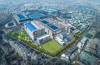 Another key benefit of 5 nm is that we can reuse all the 7 nm intellectual property (IP) to 5nm. Thereby 7 nm customers' transitioning to 5 nm will greatly benefit from reduced migration costs, pre-verified design ecosystem, and consequently shorten their 5 nm product development.
As a result of the close collaboration between Samsung Foundry and its 'Samsung Advanced Foundry Ecosystem (SAFE )' partners, a robust design infrastructure for Samsung's 5 nm, including the process design kit (PDK), design methodologies (DM), electronic design automation (EDA) tools, and IP, has been provided since the fourth quarter of 2018. Besides, Samsung Foundry has already started offering 5nm Multi Project Wafer (MPW) service to customers.
"In successful completion of our 5 nm development, we've proven our capabilities in EUV-based nodes," said Charlie Bae, Executive Vice President of Foundry Business at Samsung Electronics. "In response to customers' surging demand for advanced process technologies to differentiate their next-generation products, we continue our commitment to accelerating the volume production of EUV-based technologies."
In October 2018, Samsung announced the readiness and its initial production of 7 nm process, its first process node with EUV lithography technology. The company has provided commercial samples of the industry's first EUV-based new products and has started mass production of 7 nm process early this year.
Also, Samsung is collaborating with customers on 6 nm, a customized EUV-based process node, and has already received the product tape-out of its first 6nm chip.
Mr. Bae continued, "Considering the various benefits including PPA and IP, Samsung's EUV-based advanced nodes are expected to be in high demand for new and innovative applications such as 5G, artificial intelligence (AI), high performance computing (HPC), and automotive. Leveraging our robust technology competitiveness including our leadership in EUV lithography, Samsung will continue to deliver the most advanced technologies and solutions to customers."
Samsung foundry's EUV-based process technologies are currently being manufactured at the S3-line in Hwaseong, Korea. Additionally, Samsung will expand its EUV capacity to a new EUV line in Hwaseong, which is expected to be completed within the second half of 2019 and start production ramp-up for next year.
Compared to 7 nm, Samsung's 5 nm FinFET process technology provides up to a 25 percent increase in logic area efficiency with 20 percent lower power consumption or 10 percent higher performance as a result of process improvement to enable us to have more innovative standard cell architecture. In addition to power performance area (PPA) improvements from 7 nm to 5 nm, customers can fully leverage Samsung's highly sophisticated EUV technology. Like its predecessor, 5 nm uses EUV lithography in metal layer patterning and reduces mask layers while providing better fidelity.

As a result of the close collaboration between Samsung Foundry and its 'Samsung Advanced Foundry Ecosystem (SAFE )' partners, a robust design infrastructure for Samsung's 5 nm, including the process design kit (PDK), design methodologies (DM), electronic design automation (EDA) tools, and IP, has been provided since the fourth quarter of 2018. Besides, Samsung Foundry has already started offering 5nm Multi Project Wafer (MPW) service to customers.
"In successful completion of our 5 nm development, we've proven our capabilities in EUV-based nodes," said Charlie Bae, Executive Vice President of Foundry Business at Samsung Electronics. "In response to customers' surging demand for advanced process technologies to differentiate their next-generation products, we continue our commitment to accelerating the volume production of EUV-based technologies."
In October 2018, Samsung announced the readiness and its initial production of 7 nm process, its first process node with EUV lithography technology. The company has provided commercial samples of the industry's first EUV-based new products and has started mass production of 7 nm process early this year.
Also, Samsung is collaborating with customers on 6 nm, a customized EUV-based process node, and has already received the product tape-out of its first 6nm chip.
Mr. Bae continued, "Considering the various benefits including PPA and IP, Samsung's EUV-based advanced nodes are expected to be in high demand for new and innovative applications such as 5G, artificial intelligence (AI), high performance computing (HPC), and automotive. Leveraging our robust technology competitiveness including our leadership in EUV lithography, Samsung will continue to deliver the most advanced technologies and solutions to customers."
Samsung foundry's EUV-based process technologies are currently being manufactured at the S3-line in Hwaseong, Korea. Additionally, Samsung will expand its EUV capacity to a new EUV line in Hwaseong, which is expected to be completed within the second half of 2019 and start production ramp-up for next year.
14 Comments on Samsung Successfully Completes 5nm EUV Development
Its the same as what TSMC announced earlier this month.
There are 3 levels of production;
What do you mean by 7nm production start being distant from EUV? Samsung's 7nm has been EUV from the beginning and that was a large factor in their 7nm being ready later than TSMC's.
A big problem with EUV today is that the equipment literally cannot be manufactured fast enough. Samsung has bought basically the entire production for a couple years now, TSMC and Intel are fighting for the scraps and who is getting the equipment next :)
Oh well, 7nm TSMC would destroy them too at this point..
.
.
.
And then 10 of hysterical laughing?? :laugh::laugh::laugh::laugh::laugh:
PS: Jesus! If I play nice, I might even turn the medium into 4chan. Just need more instigating rabble and the right stir pot.