Wednesday, September 30th 2009

NVIDIA GT300 ''Fermi'' Detailed

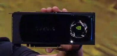
NVIDIA's upcoming flagship graphics processor is going by a lot of codenames. While some call it the GF100, others GT300 (based on the present nomenclature), what is certain that the NVIDIA has given the architecture an internal name of "Fermi", after the Italian physicist Enrico Fermi, the inventor of the nuclear reactor. It doesn't come as a surprise, that the codename of the board itself is going to be called "reactor", according to some sources.

Based on information gathered so far about GT300/Fermi, here's what's packed into it:
  • Transistor count of over 3 billion
  • Built on the 40 nm TSMC process
  • 512 shader processors (which NVIDIA may refer to as "CUDA cores")
  • 32 cores per core cluster
  • 384-bit GDDR5 memory interface
  • 1 MB L1 cache memory, 768 KB L2 unified cache memory
  • Up to 6 GB of total memory, 1.5 GB can be expected for the consumer graphics variant
  • Half Speed IEEE 754 Double Precision floating point
  • Native support for execution of C (CUDA), C++, Fortran, support for DirectCompute 11, DirectX 11, OpenGL 3.1, and OpenCL
Update: Here's an image added from the ongoing public webcast of the GPU Technology Conference, of a graphics card based on the Fermi architecture.
Source: Bright Side of News
Add your own comment

205 Comments on NVIDIA GT300 ''Fermi'' Detailed

#201
El Fiendo
imperialreignNvidia will implement a top-to-bottom release strategy from high end to entry level. (the claim that is being disputed) While he didn't talk about it during the keynote presentation meaning, Fud states that Jensen DID NOT mention the GT300 release strategy during his keynote address), this release strategy also includes a high end dual-GPU configuration that should ship around the same time ("around the same time" - meaning "not at the same time, but possibly within a month or two") as the high end single-GPU model (which contradicts the first sentence in this sentence, in that the dual-GPU will not ship at the same time as the single-GPU . . . which means it won't be a "top-to-bottom" release, as the dual-GPU would be released first).
Hold up a second. Mind your periods and commas. As that article is written it says:

Nvidia will implement a top-to-bottom release strategy from high end to entry level. <<END>> While he didn't talk about it during the keynote presentation, this release strategy also includes a high end dual-GPU configuration that should ship around the same time... <-THIS is what is implied he didn't talk about due to the way the sentence is structured. If it was saying he didn't talk about the release strategy, it would read:

Nvidia will implement a top-to-bottom release strategy from high end to entry level, even though he didn't talk about it during the keynote presentation.

Commas can change context very easily.

As for the "around the same time" - meaning "not at the same time, but possibly within a month or two" part, the quote you provide never said it would be released immediately. It only ever says 'around the same time' so nothing is contradicting.
Posted on Reply
#202
Benetanegia
El FiendoHold up a second. Mind your periods and commas. As that article is written it says:

Nvidia will implement a top-to-bottom release strategy from high end to entry level. <<END>> While he didn't talk about it during the keynote presentation, this release strategy also includes a high end dual-GPU configuration that should ship around the same time... <-THIS is what is implied he didn't talk about due to the way the sentence is structured. If it was saying he didn't talk about the release strategy, it would read:

Nvidia will implement a top-to-bottom release strategy from high end to entry level, even though he didn't talk about it during the keynote presentation.

Commas can change context very easily.

As for the "around the same time" - meaning "not at the same time, but possibly within a month or two" part, the quote you provide never said it would be released immediately. It only ever says 'around the same time' so nothing is contradicting.
Thanks, thanks. I was going to write exactly the same, but since my first language is not english, he would still have something to say about it. Thanks, thanks a lot again. Also important for the context is the previous line to what imperial posted:
However, one thing that he has confirmed is that Fermi architecture is very scalable and that it will end up in many GPUs.

so

Nvidia will implement a top-to-bottom release strategy from high end to entry level.<<END>> While he didn't talk about it during the keynote presentation, this release strategy also includes a high end dual-GPU configuration that should ship around the same time...
Posted on Reply
#203
PP Mguire
ZubasaThere never is and never will be a dual GT200 card. :nutkick:
You need to get your facts right, before you argue.
The GTX 295 is a dual GT200b card, the 55nm die shink allow this to happen.
If they try to get dual GT200 on a single cooler, you get another Asus Mars furnace.
I am sure it would have made you a cup of coffee. :roll:
Symantics. The point is everybody argued against a GTX295 type card and there was one.
Any video card that properly makes me a cup of coffee has my vote. :toast:
Posted on Reply
#204
jaredpace
The NV GF100 card looks 1000 times better than the HDbatmobileX2
Posted on Reply
#205
amschip
BenetanegiaIt depends. This is the average of all games performance at 2560x1600 from Wizzard's HD5870 review.

img.techpowerup.org/091001/perfrel_2560.gif

Compared to HD5870 the GTX285 is doing 78% and HD4870 is doing 50%, if we normalize 50% to being 100% and take it as the base, then:

78/50 * 100 = 156%

That is at 2560x1600 the GTX285 is 56% faster than HD4870 in the average of all the games that Wizzard reviews.

But wait!! Ati had another 956 million transistor card, using the same chip the HD4850, we apply the same math and that gives us that GTX285 is 95% faster or almost twice as fast. 40% more transistors and 2x the performance not too shaby isn't it? GTX285's clock is 648 Mhz, HD4870 is 750 Mhz and HD4850 is 625 Mhz.

Comparing the card at 2560x1600 does make sense, because a lot of that extra 40% transistors went to the extra 16 ROPs that help at that resolution.

What I mean with all this is, it depends.
Correct me if I'm wrong but don't you thing comparing 1GB and 512MB cards at such a high resolution is seriously flawed? If you compare gtx295 and 4870x2 both with more or less 2GB of memory the difference is not that big. The difference is only 12%. So almost 3 Billion transistors is only 12% faster than 2 Billion.
Posted on Reply
Add your own comment
May 16th, 2024 11:18 EDT change timezone

New Forum Posts

Popular Reviews

Controversial News Posts