Sunday, November 13th 2011

AMD FM1 and FM2 Packages Pictured Side-by-Side, Incompatible
Here is the first picture of AMD accelerated processing units in the existing FM1 package and future FM2 package on which the next-generation Trinity APU will be based on. Both packages are very similar, follow AMD's favourite yet archaic PGA design. The pins are physically arranged in a mostly similar fashion, though we don't have a pin map at hand. The difference comes with some of the blanked pins in the sub-central portion of the pin array. The FM2 package has 904 pins, compared to 905 on FM1. One pin is blanked, while a pair of blanked pins are arranged further away from the central cutout.
This makes FM1 and FM2 clearly incompatible. Neither will you be able to use today's A-Series APUs in the FM1 package on future socket FM2 motherboards, nor will you be able to run future FM2 APUs on today's FM1 motherboards. Yet, AMD will port the A75 FCH chipset to the next-generation "Virgo" platform. The FCH or Fusion Controller Hub, like Intel's PCH (Platform Controller Hub), is not much more than a glorified southbridge, and is portable between Fusion platforms as it's essentially a PCI-Express 2.0 x4 device. In the picture below, "Llano" FM1 APU is on the left, and "Trinity" FM2 on the right.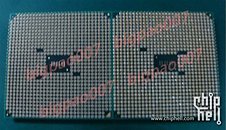
Source:
ChipHell
This makes FM1 and FM2 clearly incompatible. Neither will you be able to use today's A-Series APUs in the FM1 package on future socket FM2 motherboards, nor will you be able to run future FM2 APUs on today's FM1 motherboards. Yet, AMD will port the A75 FCH chipset to the next-generation "Virgo" platform. The FCH or Fusion Controller Hub, like Intel's PCH (Platform Controller Hub), is not much more than a glorified southbridge, and is portable between Fusion platforms as it's essentially a PCI-Express 2.0 x4 device. In the picture below, "Llano" FM1 APU is on the left, and "Trinity" FM2 on the right.

30 Comments on AMD FM1 and FM2 Packages Pictured Side-by-Side, Incompatible