Tuesday, October 2nd 2018

EVGA Also Teases Possible Z390 DARK Motherboard

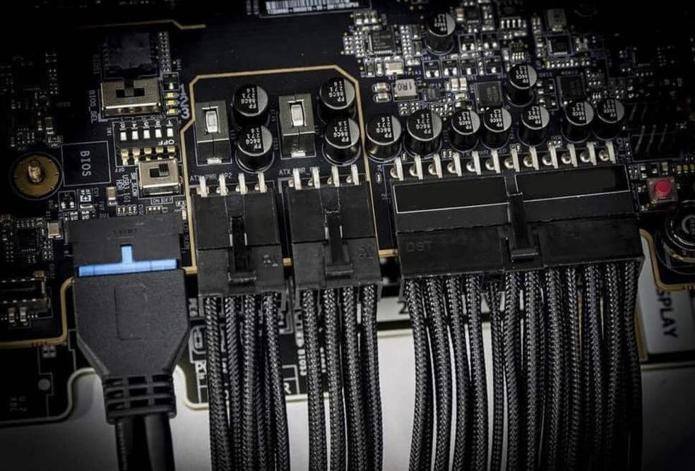
It's been a busy past 48 hours at EVGA, with the launch of the B360 Micro motherboard, unveiling of the NVLink bridges, and now a teaser of what could very well be the company's Z390 DARK motherboard, targeted at professional overclockers. K|ngp|n shared this teaser image of the board on social media, revealing a socket LGA1151 motherboard that's laid out like an LN2 overclocker's dream - memory slots north of the CPU sockets, CPU VRM to its west and south, and power drawn from a combination of 24-pin ATX and two 8-pin EPS connectors angled away toward the east. A cluster of 7-segment LED displays put out diagnostic codes. The designers seem to have opted for an expensive 8~10-layer PCB that's rich in copper. We'll hear more about this beauty as the Z390 platform launches later this month.
Add your own comment

25 Comments on EVGA Also Teases Possible Z390 DARK Motherboard

#1
agent_x007
Isn't Dual 8-pin a bit overkill for LGA 1151 socket ?
Posted on Reply
#2
dj-electric
agent_x007Isn't Dual 8-pin a bit overkill for LGA 1151 socket ?
Yes, it kinda is under any ambient cooling. An 8+4 would do the job for the toughest of overclockers under those conditions.
I'm afraid EVGA wants the attention of extremist with this.

That mentioned - really really dig this design. This is how it should have been done for years now.
Posted on Reply
#4
HELLSMAN
They making something to compete with the ROG APEX? looks that way with the two RAM slots.
Posted on Reply
#5
E-curbi
agent_x007Isn't Dual 8-pin a bit overkill for LGA 1151 socket ?
I'd say yes, for ambient cooling.

I'm using a Maximus 10 Apex and only a single 8-pin for CPU PWR and have ZERO stability issues until about 5.5Ghz - 5.6Ghz.

More likely the limitations of my Noctua air cooler, or my limited knowledge base, than the CPU power cables. lol :)
Posted on Reply
#6
bonehead123
IF you truly wanna call it a "darK' mobo, get rid of ANY and ALL coloring,,,,, the pcb traces, connection points, the yellow trim pieces etc ect....

as in BLACK, everywhere, all over, under and around everything, including the CPU clamp arm and socket too....

Otherwise it might as well be called an "almost dark" design :D
Posted on Reply
#7
DR4G00N
agent_x007Isn't Dual 8-pin a bit overkill for LGA 1151 socket ?
Well, it's pretty common to see two 8-pins on boards made for LN2 OC'ing.
Posted on Reply
#8
zo0lykas
I very like this idea, and hope so another brands notice that and do the same.

"24-pin ATX and two 8-pin EPS connectors angled away toward the east"
Posted on Reply
#9
agent_x007
DR4G00NWell, it's pretty common to see two 8-pins on boards made for LN2 OC'ing.
Sure... on HEDT (which actually needs it), or for decoration (because MOSFETs/Chokes used on PCB simply can't take that many Amps being pushed through them [600W/Vcore/Choke count for Vcore vs. it's rating]).
Regardless, I'm concerned about low pin count socket taking that many amps through it's tiny pins (in short, I'm worried about Amps/pin with OC'ed 8 Core CPU).
In past, Quad Core CPUs simply weren't capable of requiring that many Amps (not since LGA 775, but that has bigger pins).
However, for socket desinged around Quad Core Skylake, they now release a OC capable Octa Core CPU ?
(old boards do support Octa core with UEFI update, right ?)
Posted on Reply
#10
Crazy zookeepster
It seems that the CPU and ram slots have rotated as well? Id assume the ram is the upper most part of the board, then cpu socket, VRM and pci e slots thereafter? It leads to one hell of an exciting design, and kudos to EVGA for being different in this RGB unicorn porridge barf. Really looking forward to see how this turns out
Posted on Reply
#11
DR4G00N
agent_x007Sure... on HEDT (which actually needs it), or for decoration (because MOSFETs/Chokes used on PCB simply can't take that many Amps being pushed through them [600W/Vcore/Choke count for Vcore vs. it's rating]).
Regardless, I'm concerned about low pin count socket taking that many amps through it's tiny pins (in short, I'm worried about Amps/pin with OC'ed 8 Core CPU).
In past, Quad Core CPUs simply weren't capable of requiring that many Amps (not since LGA 775, but that has bigger pins).
However, for socket desinged around Quad Core Skylake, they now release a OC capable Octa Core CPU ?
(old boards do support Octa core with UEFI update, right ?)
I just meant that it was common not that it's actually needed.
In terms of amps/pin I'm going to say it's a non-issue because I trust that Intel knows what their doing when it comes to CPU's. :)

And yes, it can work on older boards. I know the 8-core works fine on the Z170M OCF though we'll have to wait and see if Nick decides to publicly provide an updated bios for it.
Posted on Reply
#12
MrFrogSD
I have always liked the horizontally oriented power, and many other, connectors. Why don't more brands do this? My guess would be cost, but as a non-industrial engineer, I can't see why it would be more expensive.
Posted on Reply
#13
Upgrayedd
herliTz1337Dark RGB or Dark dark? No RGB no buy!
I hope this is a troll attempt..its just hard to tell anymore
Posted on Reply
#14
looniam
agent_x007Sure... on HEDT (which actually needs it), or for decoration (because MOSFETs/Chokes used on PCB simply can't take that many Amps being pushed through them [600W/Vcore/Choke count for Vcore vs. it's rating]).
Regardless, I'm concerned about low pin count socket taking that many amps through it's tiny pins (in short, I'm worried about Amps/pin with OC'ed 8 Core CPU).
In past, Quad Core CPUs simply weren't capable of requiring that many Amps (not since LGA 775, but that has bigger pins).
However, for socket desinged around Quad Core Skylake, they now release a OC capable Octa Core CPU ?
(old boards do support Octa core with UEFI update, right ?)
you haven't been around LN2 much?
use 4.7Mhz + 1.35v =95 watts. compare to 6.8Mhz (45% increase [linear]) + 1.86 (88% increase [exponential!]) = 397 watts.

even if a single 8 pin can handle that, there will be a huge difference in ripple than using two 8 pin connectors that will effect stability.

i can't count how many times people complained about their graphics card getting flaky gaming/benchmarking until they used two cables instead on one w/daisy chained connectors.

now you know.

yeah my napkin math isn't perfect but it's close enough for government work.
Posted on Reply
#15
colin_mc
They still won't enable to set LLC on different levels and make shitty fan control? ;) (like in Z370 series)
Posted on Reply
#16
phill
Some boards been having those 2 8 pin CPU connectors on as far as I can remember... Both on the EVGA Classifieds and they where brilliant for Sub Zero work :) Still, love these EVGA boards and the Asrock OCF boards... Can just spend so much money thinking of the hardware you'd like let alone actually getting around to buying stuff lol I ain't gonna win :( :)
Posted on Reply
#17
agent_x007
looniamyou haven't been around LN2 much?
use 4.7Mhz + 1.35v =95 watts. compare to 6.8Mhz (45% increase [linear]) + 1.86 (88% increase [exponential!]) = 397 watts.

even if a single 8 pin can handle that, there will be a huge difference in ripple than using two 8 pin connectors that will effect stability.
It's true I didn't do LN2 (or seen anyone do it live at this point).
However, here's the limitation of "TDP" rating...
Please explain to me, how a Hex Core CPU and Octa Core CPU can pull the same ammount of power, when they are made using the same technology/architecture ?
Also, I'm worried about sockets being damaged after Octa Core OC, because of too high Amps per pin IN THE SOCKET (NOT on EPS connector).
Posted on Reply
#18
DR4G00N
agent_x007It's true I didn't do LN2 (or seen anyone do it live at this point).
However, here's the limitation of "TDP" rating...
Please explain to me, how a Hex Core CPU and Octa Core CPU can pull the same ammount of power, when they are made using the same technology/architecture ?
Also, I'm worried about sockets being damaged after Octa Core OC, because of too high Amps per pins IN THE SOCKET (NOT on EPS connector).
en.wikipedia.org/wiki/Thermal_design_power

TDP has nothing to do with the amount of power a component will use, it is rather used to determine the required level of cooling required for it to function at stock frequencies and voltages under normal workloads.
When compared stock vs. stock the 8-core will most likely use more power than the 6-core yet may not require a higher capacity heatsink to function below it's TjMax in normal workloads.

Basically TDP doesn't really mean anything to the end user and should not really be used to compare CPU's.
Posted on Reply
#19
looniam
agent_x007It's true I didn't do LN2 (or seen anyone do it live at this point).
However, here's the limitation of "TDP" rating...
Please explain to me, how a Hex Core CPU and Octa Core CPU can pull the same ammount of power, when they are made using the same technology/architecture ?
Also, I'm worried about sockets being damaged after Octa Core OC, because of too high Amps per pins IN THE SOCKET (NOT on EPS connector).
you already got an answer for one those questions:
In terms of amps/pin I'm going to say it's a non-issue because I trust that Intel knows what their doing when it comes to CPU's. :)
however, there was news making the rounds that Intel added more VSS (ground) and VCC (power) pins for 8th Gen CPUs. , they were "reserved" before, which is interesting since i had assumed they were all being used already. this was a reason intel released a new chipset - according to them.

and the TDP is simple; intel cheats. they pick an arbitrary number to make themselves look good. for one generation they may consider voltage at base clock for TDP and another voltage at all core boost clock. though it's more of an efficiency number, it is correlated to power consumption; because it has to consume power to produce heat; physics!.

like i said before; close enough for government work. ;)

seriously, i showed you it isn't a concern, HWBOT is loaded with folks pushing those sockets w/o any problems. i mean, you don't seem to wanting to push it that far, so why the concern?

let the folks who are worry about that. :)

E: and again there will be less ripple in the power going to the VRMS/socket/chip with two connectors than w/one. <- the BIG reason!
Posted on Reply
#20
londiste
zo0lykasI very like this idea, and hope so another brands notice that and do the same.
"24-pin ATX and two 8-pin EPS connectors angled away toward the east"
Oh yeah!
Not so sure about the naked legs on these connectors though.
looniamand the TDP is simple; intel cheats. they pick an arbitrary number to make themselves look good. for one generation they may consider voltage at base clock for TDP and another voltage at all core boost clock.
Regarding generational changes - so does everyone else. It is not so much Intel cheating than motherboard manufacturers cheating (WTF is MCE and friends?) and nobody reading the documentation. Intel has very good documentation on what is what and how power management works.
Posted on Reply
#21
looniam
londisteRegarding generational changes - so does everyone else. It is not so much Intel cheating than motherboard manufacturers cheating (WTF is MCE and friends?) and nobody reading the documentation. Intel has very good documentation on what is what and how power management works.
you're mixing motherboard reviews with intel's chip binning which has nothing to do with intel's:
Thermal Design Power. The thermal design power is the maximum power a processor can draw for a thermally significant period while running commercially useful software. The constraining conditions for TDP are specified in the notes in the thermal and power tables.
what the significant time period or what intel considers commercially useful software is not disclosed. it could be running handbrake for 2 minutes to web browsing for an hour; giving a vague description of the testing conditions is not reliable.

so yes, you can unknowing think they are providing information when in fact it is little to go on. don't try this, "oh it's there, people don't know how to read bullcrap."
Posted on Reply
#22
londiste
looniamwhat the significant time period or what intel considers commercially useful software is not disclosed. it could be running handbrake for 2 minutes to web browsing for an hour; giving a vague description of the testing conditions is not reliable.
You can fault Intel for a lot of things but not for the lack of proper documentation.
www.intel.com/content/dam/www/public/us/en/documents/datasheets/8th-gen-core-family-datasheet-vol-1.pdf
Page 64: 3.3.2. Intel Turbo Boost Technology 2.0
Page 88: 5. Thermal Management
Page 89: 5.1.3.1 Package Power Control
Page 102: Table 5-5. TDP Specifications (S-Processor Line)
Page 105: Table 5-7. Package Turbo Specifications (S-Processor Lines)
Regarding tables, for example 8700K is 6-Core GT2 95W.

Their test conditions do not actually account for the load. Both control as well as testing is based on power sensors (and thermal sensors which should not be a problem given adequate cooling solution).
Posted on Reply
#23
looniam
londisteYou can fault Intel for a lot of things but not for the lack of proper documentation.
www.intel.com/content/dam/www/public/us/en/documents/datasheets/8th-gen-core-family-datasheet-vol-1.pdf
Page 64: 3.3.2. Intel Turbo Boost Technology 2.0
Page 88: 5. Thermal Management
Page 89: 5.1.3.1 Package Power Control
Page 102: Table 5-5. TDP Specifications (S-Processor Line)
Page 105: Table 5-7. Package Turbo Specifications (S-Processor Lines)
Regarding tables, for example 8700K is 6-Core GT2 95W.
Their test conditions do not actually account for the load. Both control as well as testing is based on power sensors (and thermal sensors which should not be a problem given adequate cooling solution).
and that is exactly what i am getting at that you are ignoring.

since you have proved what i said yourself, we are done here. good talk.
Posted on Reply
#24
londiste
What do you mean? Why would they need to account for the load on the technical side of how things are managed? CPUs will run at full load on the specced base clock under TDP. Generally, it will run at higher than that, on the boost clock. Intel CPUs fall down to base clock primarily wih AVX or power virus (their own phrase) type of load. The limiting factor is TDP. So they follow both power consumption and temperature. That is an industry practice thing to make sure chip power consumption and cooling would be predictable.

Desktop CPUs are very well optimized to the TDP points so that TDP is not severely restricting performance. Low-power (45W, 35W) and mobile chips are where TDP restriction becomes very noticeable.
Posted on Reply
#25
looniam
i am not about to clutter up a thread thats PR on a mobo trying to explain to you some basic valid testing conditions. you even pointed out the cpu will adjust to conditions when under load such as going to max 4/6 core boost to base clock, intel not specifying those gives them wiggle room to move the goal posts when they need to.
Intel says chip vendors' TDP figures are not comparable
Not only did King say that TDP values are not transferable between chip vendors, he added that TDP figures cannot be compared between Atom and Core processors. He said, "You should note that the Atom processors use a different definition of TDP [than Core processors], one that is more oriented towards mainstream or consumption oriented workloads."
so you have it backwards, the cpu isn't very well optimized for the TDP but the TDP is adjusted for the cpu. this has been pointed out for over 11 years, since conroe, that i am aware of and some googling will show even further back than that. so what ever you say or think is not going to change history.

i am now out of time and any desire to continue this discussion here.

have a good day.
Posted on Reply
Add your own comment
Apr 19th, 2024 21:36 EDT change timezone

New Forum Posts

Popular Reviews

Controversial News Posts