Tuesday, August 27th 2019
Cerebras Systems' Wafer Scale Engine is a Trillion Transistor Processor in a 12" Wafer
This news isn't properly today's, but it's relevant and interesting enough that I think warrants a news piece on our page. My reasoning is this: in an era where Multi-Chip Modules (MCM) and a chiplet approach to processor fabrication has become a de-facto standard for improving performance and yields, a trillion-transistor processor that eschews those modular design philosophies is interesting enough to give pause.
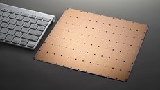
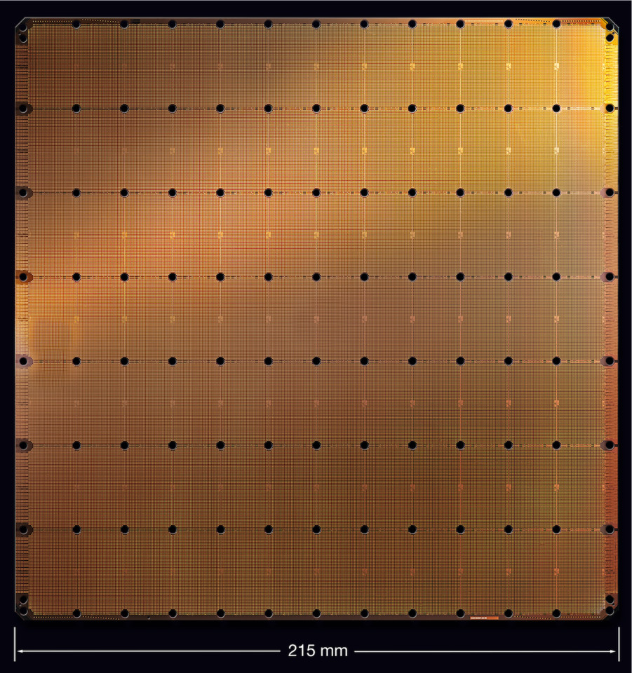
The Wafer Scale engine has been developed by Cerebras Systems to face the ongoing increase in demand for AI-training engines. However, in workloads where latency occur a very real impact in training times and a system's capability, Cerebras wanted to design a processor that avoided the need for a communication lane for all its cores to communicate - the system is only limited, basically, by transistors' switching times. Its 400,000 cores communicate seamlessly via interconnects, etched on 42,225 square millimeters of silicon (by comparison, NVIDIA's largest GPU is 56.7 times smaller at "just" 815 square millimeters).
 However, in a world where silicon wafer manufacturing still has occurrences of manufacturing defects that can render whole chips inoperative, how did Cerebras manage to build such a large processor and keep it from having such defects that it can't actually deliver on the reported specs and performance? The answer is an old one, mainly: redundancy, paired with some additional magical engineering powders achieved in conjunction with the chips' manufacturer, TSMC. The chip is built on TSMC's 16 nm node - a more refined process with proven yields, cheaper than a cutting-edge 7 nm process, and with less areal density - this would make it even more difficult to properly cool those 400,000 cores, as you may imagine.
Cross-reticle connectivity, yield, power delivery, and packaging improvements have all been researched and deployed by Cerebras in solving the scaling problems associated with such large chips. moreover, the chips is built with redundant features that should ensure that even if some defects arise in various parts of the silicon chip, the areas that have been designed as "overprovisioning" can cut in an pick up the slack, routing and processing data without skipping a beat. Cerebras says any given component (cores, SRAM, etc) of the chip features 1%, 1.5% of additional overprovisioning capability that enables any manufacturing defects to be just a negligible speedbump instead of a silicon-waster. The inter-core communication solution is one of the most advanced ever seen, with a fine-grained, all-hardware, on-chip mesh-connected communication network dubbed Swarm that delivers an aggregate bandwidth of 100 petabits per second.. this is paired with 18 Gb of local, distributed, superfast SRAM memory as the one and only level of the memory hierarchy - delivering memory bandwidth in the realm of 9 petabytes per second.
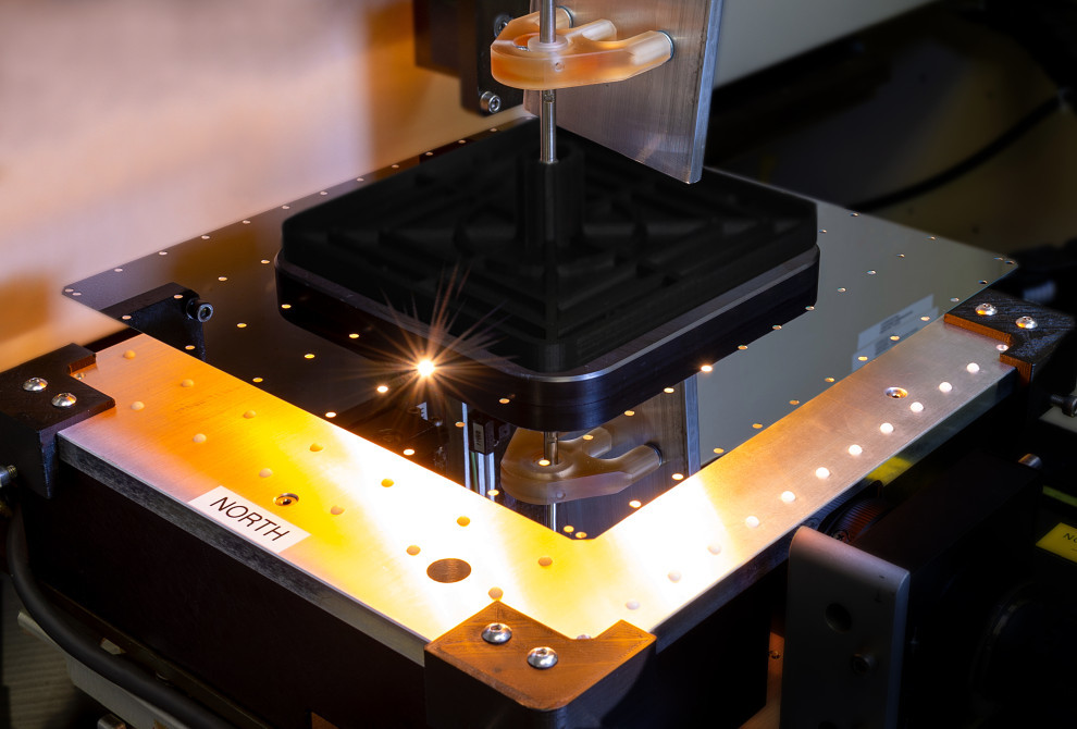
The 400,000 cores are custom-designed for AI workload acceleration. Named SLAC for Sparse Linear Algebra Cores, these are flexible, programmable, and optimized for the sparse linear algebra that underpins all neural network computation (think of these as FPGA-like, programmable arrays of cores). SLAC's programmability ensures cores can run all neural network algorithms in the constantly changing machine learning field - this is a chip that can adapt to different workloads and AI-related problem solving and training - a requirement for such expensive deployments as the Wafer Scale Engine will surely pose. The entire chip and its accompanying deployment apparatus had to be developed in-house. As founder and CEO Andrew Feldman puts it, there were no packaging, printed circuit boards, connectors, cold plates, tools or any software that could be adapted towards the manufacturing and deployment of the Wafer Scale Engine. This means that Cerebras Systems' and its team of 173 engineers had to develop not only the chip, but almost everything else that is needed to make sure it actually works. The Wafer Scale Engine consumes 15 kilowatts of power to operate - a prodigious amount of power for an individual chip, although relatively comparable to a modern-sized AI cluster. This is a cluster, in essence, but deployed in a solo chip with none of the latency and inter-chip communication hassles that plague clusters.
In an era where companies are looking towards chiplet design and inter-chip communication solutions as ways to tackle the increasing challenges of manufacturing density and decreasing yields, Cerebras' effort proves that there is still a way of developing monolithic chips that place performance above all other considerations.
Sources:
VentureBeat, TechCrunch
The Wafer Scale engine has been developed by Cerebras Systems to face the ongoing increase in demand for AI-training engines. However, in workloads where latency occur a very real impact in training times and a system's capability, Cerebras wanted to design a processor that avoided the need for a communication lane for all its cores to communicate - the system is only limited, basically, by transistors' switching times. Its 400,000 cores communicate seamlessly via interconnects, etched on 42,225 square millimeters of silicon (by comparison, NVIDIA's largest GPU is 56.7 times smaller at "just" 815 square millimeters).


Cross-reticle connectivity, yield, power delivery, and packaging improvements have all been researched and deployed by Cerebras in solving the scaling problems associated with such large chips. moreover, the chips is built with redundant features that should ensure that even if some defects arise in various parts of the silicon chip, the areas that have been designed as "overprovisioning" can cut in an pick up the slack, routing and processing data without skipping a beat. Cerebras says any given component (cores, SRAM, etc) of the chip features 1%, 1.5% of additional overprovisioning capability that enables any manufacturing defects to be just a negligible speedbump instead of a silicon-waster.
The 400,000 cores are custom-designed for AI workload acceleration. Named SLAC for Sparse Linear Algebra Cores, these are flexible, programmable, and optimized for the sparse linear algebra that underpins all neural network computation (think of these as FPGA-like, programmable arrays of cores). SLAC's programmability ensures cores can run all neural network algorithms in the constantly changing machine learning field - this is a chip that can adapt to different workloads and AI-related problem solving and training - a requirement for such expensive deployments as the Wafer Scale Engine will surely pose.

In an era where companies are looking towards chiplet design and inter-chip communication solutions as ways to tackle the increasing challenges of manufacturing density and decreasing yields, Cerebras' effort proves that there is still a way of developing monolithic chips that place performance above all other considerations.
20 Comments on Cerebras Systems' Wafer Scale Engine is a Trillion Transistor Processor in a 12" Wafer
I do wonder how will system integration work, however. The chip is quite large and integrating something like that on a PCB would be difficult. Also, expansion of the chip is quite possible due to the huge amount of heat. Can't wait to see how will they solve those problems
And it is not a simple solution either since they not only had to solve the problem at hand but also design new advanced tools and software to actually pull it off.
They also already manufactured wafers and are ready to introduce their manufacturing process to the world.
Often when you hear about new stuff like this it is only a working theory on the drawing board with 10-15 years work before final product.
15 kilowatt is a little hot BUT imagine this tech on 5nm in the future with 3 kilowatt.
Bet they already working in 3D stacking these monsters
A bit bigger in size than what we've seen on the Big Screen, but give it time and it will fit in a T-800's head.
By the story of the 3rd episode, the problem happens when Skynet is "geting out" to the internet, gaining a huge amount of compute power by "infecting" all connected devices and becoming self-conscious.
www.tomshardware.com/news/nvidia-msm-inference-chip,39780.html
interested to see how they will provide the bandwidth this needs in order to process data at capacity.
At the moment AI research may be done in a GPU with 8 GiB to 24 GiB Ram, the complete dataset might not fit in the GPU ram, so it will be done in batches.
The same way the data sets might be loaded into the internal 18 GiB memory for the new beast.
To compare a Radeon VII, it has 3840 shading units, and 1 TB/s memory access to its 16 GiB on-board Ram. This new chip has basically moved all that onto one chip, with 9 000 x the access speed and 100 x the number of cores.
A modern day GPU doing AI would be feed by the PCIe bus, a gen 4 at 16 x would be capable of 128 GB/s, since this is a basic data dump (from system memory if you wish to sustain that speed for all of the 16 GB to the GPU) it requires little to no computation and approximately 125 ms of write time.
The same way, to fill the 18 GiB of on-board memory could be accomplished in less than 5 seconds from a PCIe x 4 gen 4 NVME drive. If your computation takes 20 minutes that is not the big problem.