Thursday, May 14th 2020

NVIDIA GA100 Scalar Processor Specs Sheet Released

NVIDIA today unveiled the GTC 2020, online event, and the centerpiece of it all is the GA100 scalar processor GPU, which debuts the "Ampere" graphics architecture. Sifting through a mountain of content, we finally found the slide that matters the most - the specifications sheet of GA100. The GA100 is a multi-chip module that has the 7 nm GPU die at the center, and six HBM2E memory stacks at its either side. The GPU die is built on the TSMC N7P 7 nm silicon fabrication process, measures 826 mm², and packing an unfathomable 54 billion transistors - and we're not even counting the transistors on the HBM2E stacks of the interposer.

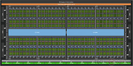
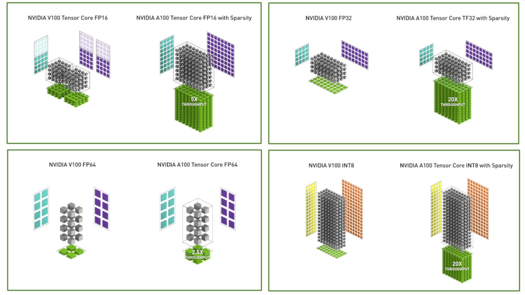
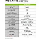
The GA100 packs 6,912 FP32 CUDA cores, and independent 3,456 FP64 (double-precision) CUDA cores. It has 432 third-generation tensor cores that have FP64 capability. The three are spread across a gargantuan 108 streaming multiprocessors. The GPU has 40 GB of total memory, across a 6144-bit wide HBM2E memory interface, and 1.6 TB/s total memory bandwidth. It has two interconnects: a PCI-Express 4.0 x16 (64 GB/s), and an NVLink interconnect (600 GB/s). Compute throughput values are mind-blowing: 19.5 TFLOPs classic FP32, 9.7 TFLOPs classic FP64, and 19.5 TFLOPs tensor cores; TF32 156 TFLOPs single-precision (312 TFLOPs with neural net sparsity enabled); 312 TFLOPs BFLOAT16 throughout (doubled with sparsity enabled); 312 TFLOPs FP16; 624 TOPs INT8, and 1,248 TOPS INT4. The GPU has a typical power draw of 400 W in the SXM form-factor. We also found the architecture diagram that reveals GA100 to be two almost-independent GPUs placed on a single slab of silicon. We also have our first view of the "Ampere" streaming multiprocessor with its FP32 and FP64 CUDA cores, and 3rd gen tensor cores. The GeForce version of this SM could feature 2nd gen RT cores.
Add your own comment

101 Comments on NVIDIA GA100 Scalar Processor Specs Sheet Released

#1
Daven
Figuring out how they get 40 GB from 6 HBM stacks is a little confusing. Some sites are reporting one or more stacks are disabled. Seems weird. My guess is that the stacks have different memory amounts. For instance, 4 stacks could have 8 GB each and 2 stacks could have 4 GB each.

Edit: Is it possible to have 1.6 GB per wafer in a stack?

Edit #2: Oh and on an unrelated note, it was just released that Nvidia is dropping Xeon and going with Epyc for its complete server solutions.
Posted on Reply
#2
dicktracy
RDNA2 should just stick to consoles.
Posted on Reply
#3
dyonoctis
If this translate to consumers GPUs, then that next gen might be comparabale to what happened with the 8800 gtx... with another price bump if AMD can't answer.
Posted on Reply
#4
RH92
Can't wait to see what a FP16 and FP32 optimised SM will look like . This might be the biggest generational leap we have ever experienced ! So the rumors of 3060 class of GPU running circles around 2080Ti especially in RTX might not be that off .
Posted on Reply
#5
Breit
Mark LittleFiguring out how they get 40 GB from 6 HBM stacks is a little confusing. Some sites are reporting one or more stacks are disabled. Seems weird. My guess is that the stacks have different memory amounts. For instance, 4 stacks could have 8 GB each and 2 stacks could have 4 GB each.

Edit: Is it possible to have 1.6 GB per wafer in a stack?

Edit #2: Oh and on an unrelated note, it was just released that Nvidia is dropping Xeon and going with Epyc for its complete server solutions.
I wondering that myself. Maybe just a typo and it should've said 48GB?
Posted on Reply
#6
ARF
dicktracyRDNA2 should just stick to consoles.
Why would anyone benefit from not having healthy competition ?
Are you willing to pay $1500 for a potential RTX 3080 Ti or would you prefer if AMD releases a $700 Navi 21 that is as fast as RTX 3080 Ti ?
Posted on Reply
#7
RH92
ARFWhy would anyone benefit from not having healthy competition ?
Are you willing to pay $1500 for a potential RTX 3080 Ti or would you prefer if AMD releases a $700 Navi 21 that is as fast as RTX 3080 Ti ?
Even better AMD releases a $300 Navi 21 that is as fast as RTX 3080 Ti ........ yeah let's not dream too much !

Jokes aside ofc i get what you mean and agree 100% competition is always good , but let's wait and see what each company has to offer this time around before making unrealistic expectations .
Posted on Reply
#8
Vya Domus
Very unimpressive FP32 and FP64 performance, I was way off in my estimations. Again, it's a case of optimizing for way too many things. So much silicon is dedicated to non traditional performance metrics that I wonder if it makes sense trying to shove everything in one package.

Here's hoping that Ampere as is in this instance wont power any consumer graphics because the outlook would be grim, we would be looking at another barley incremental performance increase.
Posted on Reply
#9
Dante Uchiha
RH92Can't wait to see what a FP16 and FP32 optimised SM will look like . This might be the biggest generational leap we have ever experienced ! So the rumors of 3060 class of GPU running circles around 2080Ti especially in RTX might not be that off .
Having ASICs/Shaders dedicated to specific tasks was not the mistake that led to the absurd prices of the Turing gen ? Let's see how much Nvidia can keep this interesting for gamers, with huge and expensive dies with low yields/waffer. It is interesting that amd's strategy with RDNA2 is precisely the opposite. :)
Posted on Reply
#10
T4C Fantasy
CPU & GPU DB Maintainer
Mark LittleFiguring out how they get 40 GB from 6 HBM stacks is a little confusing. Some sites are reporting one or more stacks are disabled. Seems weird. My guess is that the stacks have different memory amounts. For instance, 4 stacks could have 8 GB each and 2 stacks could have 4 GB each.

Edit: Is it possible to have 1.6 GB per wafer in a stack?

Edit #2: Oh and on an unrelated note, it was just released that Nvidia is dropping Xeon and going with Epyc for its complete server solutions.
1 is probably disabled because it seems to be 5120bit, this equals to be 1,555GB/s bandwidth @ 1215MHz
Posted on Reply
#12
Vya Domus
dyonoctisIt will:
www.techpowerup.com/267090/nvidia-ampere-designed-for-both-hpc-and-geforce-quadro
Sad reacts only, all those "RTX 3060 as fast as a 2080ti" seem out of this world right know. I am still hoping they'll actually increase the shader count and not just cut away the HPC oriented stuff. But damn, it just doesn't look all that enticing.

By the way I've just noticed the power :), 400W, that's 150W over V100. Ouch, 7nm hasn't been kind, I was right that this is a power hungry monster.
Posted on Reply
#13
xkm1948
Wonder whether Nvidia will introduce A100 as a standalone Titan. As nice as DGX, it is way out of budget for any single research lab. Now a few Titan A100 might be a good option for researchers to tinker with.
Posted on Reply
#14
EarthDog
ARFwould you prefer if AMD releases a $700 Navi 21 that is as fast as RTX 3080 Ti ?
I think we'd all prefer this, however, Navi 21 isn't competing with (performance wise) an RTX 3080 Ti. It will be lucky to best the 2080 Ti by a worthy (10%) margin.
Posted on Reply
#15
ppn
7nm shrink of 2080Ti +tensor a 330mm2 chip, 3080 10GB +20%clock + 10% IPC.
Posted on Reply
#16
RH92
Dante UchihaHaving ASICs/Shaders dedicated to specific tasks was not the mistake that led to the absurd prices of the Turing gen ?
For starter having fixed function silicon dedicated to specific task was everything but a mistake ! Today Nvidia is leading in raytracing and they are managing to alleviate a big part of the penalties that come with it ( reduced frame-rates ) thanks to techniques such as DLSS 2.0 which count on said fixed function silicon . This is the future of graphics and if anything else we should expect more/improved fixed function silicon with upcoming gens not the opposite , so qualifying them as a ''mistake'' means your are not understanding what the future of GPUs is , despite it being right in-front of your eyes !

About the absurd prices of Turing ( which we all agree they are ) nothing indicates that fixed function silicon is the cause for it . Quite the oposite considering from what we know fixed function silicon takes very little die space , so what makes you objectively believe this is the reason of said absurd prices ? The only objective reason is lack of competition from AMD !
Dante UchihaIt is interesting that amd's strategy with RDNA2 is precisely the opposite. :)
:shadedshu: Sorry what ? RDNA2 is going to follow the same route by implementing fixed function silicon , what are you talking about ?
Posted on Reply
#17
TheoneandonlyMrK
RH92For starter having fixed function silicon dedicated to specific task was everything but a mistake ! Today Nvidia is leading in raytracing and they are managing to alleviate a big part of the penalties that come with it ( reduced frame-rates ) thanks to techniques such as DLSS 2.0 which count on said fixed function silicon . This is the future of graphics and if anything else we should expect more/improved fixed function silicon with upcoming gens not the opposite , so qualifying them as a ''mistake'' means your are not understanding what the future of GPUs is , despite it being right in-front of your eyes !

About the absurd prices of Turing ( which we all agree they are ) nothing indicates that fixed function silicon is the cause for it . Quite the oposite considering from what we know fixed function silicon takes very little die space , so what makes you objectively believe this is the reason of said absurd prices ? The only objective reason is lack of competition from AMD !


:shadedshu: Sorry what ? RDNA2 is going to follow the same route by implementing fixed function silicon , what are you talking about ?
While I have no coin in the argument against fixed function hardware, it will be tested by time but can certainly do the job, and efficiently.
Some of what your saying is wrong ,it takes up quite a lot of die space relatively hence Nvidia's large die sizes which are added to by the requirements of extra cache resources and hardware needed to keep the special units busy.

The other reason being because they can, and to make more money, it's not rocket science just business, people should have chosen with their wallet's.

Any talk of their competition's version is hearsay at this point ,no argument required.
Posted on Reply
#18
Fluffmeister
EarthDogI think we'd all prefer this, however, Navi 21 isn't competing with (performance wise) an RTX 3080 Ti. It will be lucky to best the 2080 Ti by a worthy (10%) margin.
Yeah, it would be nice to have a 2080 Ti competitor first.
Posted on Reply
#19
TheLostSwede
News Editor
I hope we all can agree that this "leak" was a bunch of BS at least.

Posted on Reply
#20
T4C Fantasy
CPU & GPU DB Maintainer
TheLostSwedeI hope we all can agree that this "leak" was a bunch of BS at least.

Yeah GA100 is exclusive to servers\AI
GA102 will be the gaming\consumer version
Posted on Reply
#21
TheoneandonlyMrK
TheLostSwedeI hope we all can agree that this "leak" was a bunch of BS at least.

They're not releasing ga100 to consumers in any Rtx form though that's for sure.
They could be legit future specs still If you count cuda core's equally (cuda64 and cuda32 cores), perhaps.
Posted on Reply
#23
Dante Uchiha
RH92For starter having fixed function silicon dedicated to specific task was everything but a mistake ! Today Nvidia is leading in raytracing and they are managing to alleviate a big part of the penalties that come with it ( reduced frame-rates ) thanks to techniques such as DLSS 2.0 which count on said fixed function silicon . This is the future of graphics and if anything else we should expect more/improved fixed function silicon with upcoming gens not the opposite , so qualifying them as a ''mistake'' means your are not understanding what the future of GPUs is , despite it being right in-front of your eyes !

About the absurd prices of Turing ( which we all agree they are ) nothing indicates that fixed function silicon is the cause for it . Quite the oposite considering from what we know fixed function silicon takes very little die space , so what makes you objectively believe this is the reason of said absurd prices ? The only objective reason is lack of competition from AMD !


:shadedshu: Sorry what ? RDNA2 is going to follow the same route by implementing fixed function silicon , what are you talking about ?
In fact, big dies reduce the yields (functional chips/wafer) so it increases the cost of each chip and Nvidia tries to maintain profit margins to satisfy shareholders, this combination leads to high prices. I know Nvidia has managed to take advantage of the error itself, but that's questionable, as for now the results are not always consistent.

What I understand is that raytracing on RDNA2 uses a part of regular shaders. I honestly haven't seen anything about dedicated hardware.
Posted on Reply
#24
TheoneandonlyMrK
From others this is the A100 not GA100

The GA100 is the full fat 8192 GPU.
Posted on Reply
#25
T4C Fantasy
CPU & GPU DB Maintainer
theoneandonlymrkFrom others this is the A100 not GA100

The GA100 is the full fat 8192 GPU.
There is no difference, A100 is just the Tesla name it uses a GA100
Posted on Reply
Add your own comment
Apr 27th, 2024 09:20 EDT change timezone

New Forum Posts

Popular Reviews

Controversial News Posts