Monday, January 11th 2021

Dual-CCD Ryzen 5 5600X and Ryzen 7 5800X In the Wild

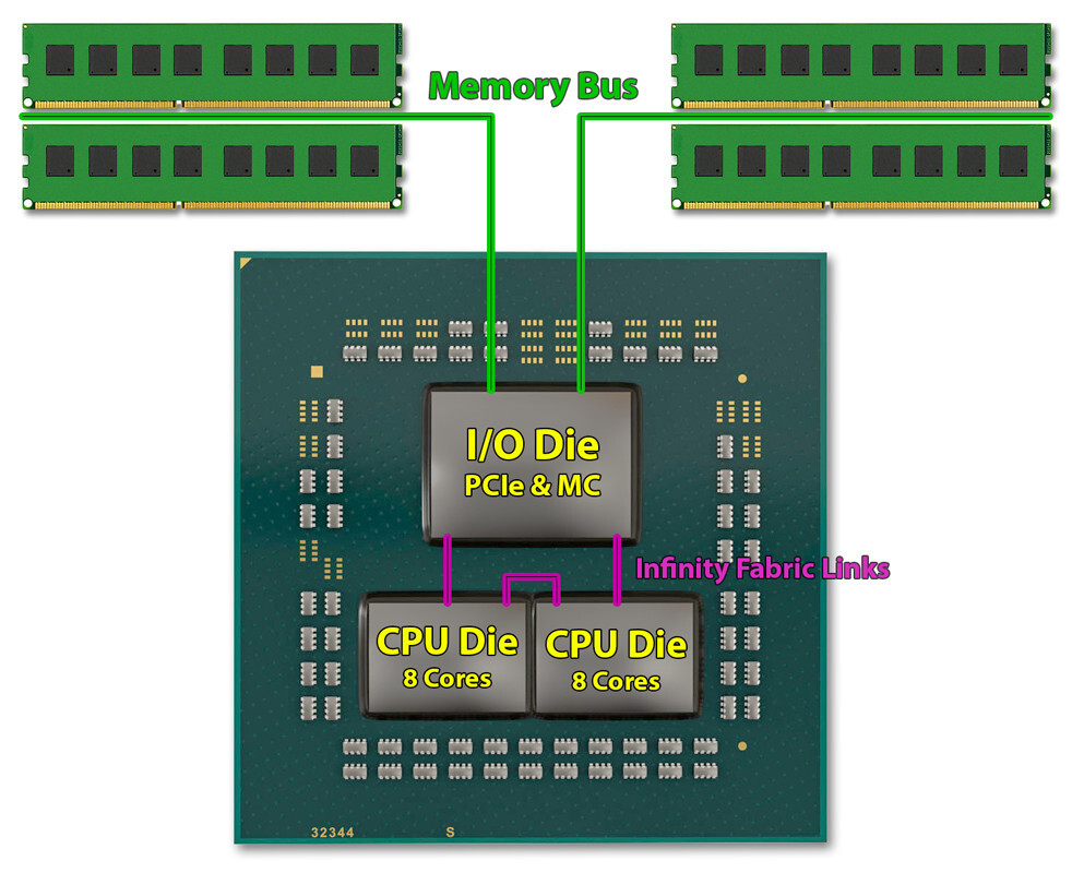
Certain AMD Ryzen 5 5600X and Ryzen 7 5800X processors are physically based on a dual-CCD design, according to an investigative report by Igor's Lab and Yuri "1usmus" Bubliy. The 5600X and 5800X are normally meant to be single-CCD processors owing to their core-counts. Based on the "Vermeer" multi-chip module design, the Ryzen 5000 series desktop processors use up to two 8-core CCDs to achieve their core-counts of up to 16 cores, with the 6-core 5600X and 8-core 5800X normally having just one CCD; while the 12-core 5900X and 16-core 5950X use two.

There are, apparently, some 5600X and 5800X built from dual-CCD MCMs, in which an entire CCD, although physically present on the package, is disabled. A 5600X based on a dual-CCD design is essentially a 5900X from which one of the CCDs didn't fully qualify; while the 5800X dual-CCD is a 5950X in which one such die didn't quite make the cut. There's no telling which CCD is disabled, it could be CCD 0 or CCD 1, those with CCD 0 disabled could trigger minor (benign) UI bugs with certain tuning utilities, which is how Wallossek and Bubliy discovered these chips. In any case, you're getting a 5600X or 5800X that works as advertised, and is fully covered by AMD's product warranties. Igor's Lab is investigating further into these dual-CCD 5600X and 5800X chips, and is probing the possibility of unlocking them to Ryzen 9.
Source: Igor's Lab
Add your own comment

62 Comments on Dual-CCD Ryzen 5 5600X and Ryzen 7 5800X In the Wild

#26
SL2
r9The real question is how to unlock those extra cores.
When we know that, the next step is to find out the weight difference of the retail boxes, i.e figuring out the number of chiplets with a scale, without opening the box. :D
Posted on Reply
#27
freeagent
r9The real question is how to unlock those extra cores.
Remember my 3 core Athlon that unlocked to 4 core Phenom II that I paid like $50 for it.
Those were good ole days.
I have a feeling those days are long gone now. I was going to buy a 5600X but now I’m leaning to 5800X. I’m getting excited :)
Posted on Reply
#28
r9
MatsWhen we know that, the next step is to find out the weight difference of the retail boxes, i.e figuring out the number of chiplets with a scale, without opening the box. :D
You have criminal mind, I like it! :D
Posted on Reply
#29
TheinsanegamerN
r9The real question is how to unlock those extra cores.
Remember my 3 core Athlon that unlocked to 4 core Phenom II that I paid like $50 for it.
Those were good ole days.
The days of 40+ PCIe lanes from the chipset, x16/x16 SLI, and crazy OCs.

I always wanted a socket AM3 system, something about the customizeability always appealed to me.
Posted on Reply
#30
Valantar
The likelihood of these being somehow unlockable is essentially zero. I would be shocked if anyone could pull that off. If a CCD is disabled, nothing in the system knows it's there, after all.
Posted on Reply
#31
TheinsanegamerN
ValantarThe likelihood of these being somehow unlockable is essentially zero. I would be shocked if anyone could pull that off. If a CCD is disabled, nothing in the system knows it's there, after all.
I mean socket AM3 processors had "disabled" cores that the system couldnt see either, didnt stop unlocking. IF the disabled CCD is still connected to the controller, there is a chance someone can unlock them. Only if they were somehow lazered after the fact would they be truly unreachable.
Posted on Reply
#32
r9
ValantarThe likelihood of these being somehow unlockable is essentially zero. I would be shocked if anyone could pull that off. If a CCD is disabled, nothing in the system knows it's there, after all.
I fear the same, but it would be a great selling point for AMD(suspect they need one ATM). Just wishful thinking on my end. :D
Posted on Reply
#33
jesdals
It would give more cache to these CPUs and I wonder if It will show better memory performance / latency wise
Posted on Reply
#34
TheoneandonlyMrK
jesdalsIt would give more cache to these CPUs and I wonder if It will show better memory performance / latency wise
Nope , the cores , cache and everything else in one of the two CCD is disabled , none of it's resources are available.
The Op States the extra CCD is dark silicon, dead to the world.
Posted on Reply
#35
Makaveli
theoneandonlymrkNope , the cores , cache and everything else in one of the two CCD is disabled , none of it's resources are available.
The Op States the extra CCD is dark silicon, dead to the world.
lol they should just sticky your response the same question getting asked over and over.
Posted on Reply
#36
kaisersolo
Is this why Ryzen Master can't see my cores or give me frequency readings on my 5600x . This issue has been report to AMD .
Posted on Reply
#37
newtekie1
Semi-Retired Folder
ValantarThe likelihood of these being somehow unlockable is essentially zero. I would be shocked if anyone could pull that off. If a CCD is disabled, nothing in the system knows it's there, after all.
The same is true with older processors that were able to be unlocked. There is obviously a method for the motherboard to communicate with the CPU and get core counts etc. And there are motherboards that let you adjust the number of active cores. So they just have to get the motherboard to override the core configuration that the CPU provides.
Posted on Reply
#38
TheoneandonlyMrK
kaisersoloIs this why Ryzen Master can't see my cores or give me frequency readings on my 5600x . This issue has been report to AMD .
Probably not ,start a thread for your issue , if the other CCD is dead ,Lazer cut or removed via other means it's still not there to the system and can't get involved in issues.
Although this isn't impossible it's unlikely.
Posted on Reply
#39
Chrispy_
TheinsanegamerNI mean socket AM3 processors had "disabled" cores that the system couldnt see either, didnt stop unlocking. IF the disabled CCD is still connected to the controller, there is a chance someone can unlock them. Only if they were somehow lazered after the fact would they be truly unreachable.
Yeah, I X4'd a couple of old X3 chips. One (Phenom II) worked flawlessly, one (Athlon) was crashtastic. It went back to being an X3

Lasering never stopped us. There was the pencil trick, and later the "short these two CPU pins with a bit of copper in the socket" tricks back in the day.
Posted on Reply
#40
Valantar
TheinsanegamerNI mean socket AM3 processors had "disabled" cores that the system couldnt see either, didnt stop unlocking. IF the disabled CCD is still connected to the controller, there is a chance someone can unlock them. Only if they were somehow lazered after the fact would they be truly unreachable.
They did, but I would be very surprised if new CPUs didn't have more advanced mechanisms for these things. A modern CPU is a lot more advanced than even one from ten years back after all. Who knows what is needed to activate an IF link on the IOD, or enable power management for a new CCD? I would be very surprised if all of this was still active, just waiting for the motherboard to say "hey, you know those cores we don't talk about? Let's use them."
Posted on Reply
#41
InVasMani
Chrispy_Ew no, the single biggest reason Zen3 is so good is because of the unified cache and lower latency that brings.
Splitting 6 or 8 cores over two CCDs is basically assembling a Zen2 CPU out of reject Zen3 parts, and everyone already has a Zen2.


Okay, I calmed down enough to read the second paragraph now.
I wonder why they're doing this? Can it really be cheaper to produce all CPUs the same dual-CCD way and just disable chips where one of them has too much damage to even make a 6-core?
Doubtful it's cheaper, but quicker to market than verifying the integrate of every core within a chip. AMD likely made the decision it's more beneficial to get chips on the market quickly at a higher price premium given the demand. Beyond that Intel isn't standing still and AMD knows as much so they probably trying to capitalize as much as possible on profits from the Ryzen architecture now. AMD taking it's sweet *** time won't do itself any favors if they wish to continue with their leading position.
Posted on Reply
#42
Fluffmeister
Nvidia definitely want a dollar for every "gimp" comment from this day forth.
Posted on Reply
#43
Wirko
ValantarThey did, but I would be very surprised if new CPUs didn't have more advanced mechanisms for these things. A modern CPU is a lot more advanced than even one from ten years back after all. Who knows what is needed to activate an IF link on the IOD, or enable power management for a new CCD? I would be very surprised if all of this was still active, just waiting for the motherboard to say "hey, you know those cores we don't talk about? Let's use them."
If I am to guess, I'd say AMD made it possible (to gain some praise from its fans) but made sure it's complicated, risky, and there's little to gain.

But ... cores aside, wouldn't it be nice if one could at least activate the L3 cache on the second chip?
Posted on Reply
#44
Valantar
WirkoIf I am to guess, I'd say AMD made it possible (to gain some praise from its fans) but made sure it's complicated, risky, and there's little to gain.

But ... cores aside, wouldn't it be nice if one could at least activate the L3 cache on the second chip?
Given that L3 caches aren't shared across CCDs, no, that would be utterly pointless. Each core only has access to the L3 in its CCX, which for Zen 2 and earlier meant 1/2 of what's on one CCD, and for Zen 3 means what's on one CCD.

I don't think AMD has any incentive to do stuff like this any more. For the old Athlon X3s, I don't think they saw any value in going to the extra expense of actually lasering off the extra cores, and the proportion of users actually unlocking anything was probably small enough to not make a difference. These days, when PC gaming has blown up and DIY PC builds are suddenly the realm of even the cool kids? Not worth the inevitable RMA hassle of people breaking their CPUs and blaming AMD for "not supporting" "features" that are at best hacks. The more time passes, the more locked-down the hardware capabilities of PCs become.
Posted on Reply
#45
Wirko
ValantarGiven that L3 caches aren't shared across CCDs, no, that would be utterly pointless. Each core only has access to the L3 in its CCX, which for Zen 2 and earlier meant 1/2 of what's on one CCD, and for Zen 3 means what's on one CCD.
The review at Anandtech seems to confirm what you're saying: there's either ~17 ns latency between cores on the same CCD, or ~82 ns between CCDs, which is DRAM latency. There's nothing in between. What I thought before is that L3 is always available to the whole CPU, regardless of topology, but with varying amount of latency.
Posted on Reply
#46
Valantar
WirkoThe review at Anandtech seems to confirm what you're saying: there's either ~17 ns latency between cores on the same CCD, or ~82 ns between CCDs, which is DRAM latency. There's nothing in between. What I thought before is that L3 is always available to the whole CPU, regardless of topology, but with varying amount of latency.
There's nothing saying that L3 has to be shared across all compute resources on the CPU/APU/SoC - that's entirely up to how the chipmaker wants to lay out their cores. Up until Zen I don't think we've ever seen split L3 designs in the consumer/enthusiast space simply because Intel uses a ring bus to connect their consumer chips and a mesh for their high core count HEDT/server stuff, so every core connects to every core there, and while each core houses a slice of L3 which it obviously has much faster access to, they're all still interconnected through a single network, and latency to non-local L3 slices should be roughly even for any given core. With the introduction of the CCX concept with Zen AMD started consistently splitting their L3 cache with each portion bound to its CCX alone, likely to keep cache latencies relatively consistent inside of the CCX. That's actually a major contributor to the performance of Zen 3: The doubling of CCX size and thus doubling of L3 cache available to each core (with IIRC next to no latency penalty, which is remarkable). Previously you had an intra-CCD latency split due to CCX-to-CCX latency too, which you can see in AT's Renoir testing.

Actually the 3950X numbers from the review you linked are really interesting, as there's no difference in latency between CCXes on the same chiplet or across them, which would suggest that either Infinity Fabric between each die has next to no latency compared to on-die IF, or that on-die CCX-to-CCX communication goes through the IOD or something similar. The latter sounds very inefficient, and the former sounds utopian, so I wonder what's the explanation there...
Posted on Reply
#47
kapone32
droopyROJust like those X3 chips all those years ago ?
Those were sweet just apply core unlock in the BIOS and you have an extra core.
Posted on Reply
#48
demi9od
Summer where is my other CCD.
Posted on Reply
#49
londiste
ValantarActually the 3950X numbers from the review you linked are really interesting, as there's no difference in latency between CCXes on the same chiplet or across them, which would suggest that either Infinity Fabric between each die has next to no latency compared to on-die IF, or that on-die CCX-to-CCX communication goes through the IOD or something similar. The latter sounds very inefficient, and the former sounds utopian, so I wonder what's the explanation there...
IIRC it has been said on-die CCX-to-CCX communication basically goes through IOD.
Posted on Reply
#50
mb194dc
Interesting find by Igor, there are other weirdies on some of the older Ryzens as well.

E.g my generation one Ryzen 5 1600 with dual channel 2666mhz ram benches at 50GB/s memory transfer rate ~ in AIDA and shows higher than expected bench in others too. Only when I overclock it on the fly using the original version of Ryzen Master. That should be impossible, theoretical max bandwidth with only 2 channels of this ram is 21.3 x 2=42.6GB.

I had wondered if there was either a bug in the benches or if that version of Ryzen Master accidentally has some code AMD should have taken out of it...
Posted on Reply
Add your own comment
Apr 26th, 2024 20:30 EDT change timezone

New Forum Posts

Popular Reviews

Controversial News Posts