Friday, February 18th 2022

Intel "Tick Tock" Alive Again, Company Announces New Intel 18A Node (1.8 nm Class)

The "tick tock" product development cycle, which enabled Intel to develop a new silicon fabrication node every alternating year, a new microarchitecture every alternating year, and interleaving the two in such a way that each new microarchitecture is built on two successive nodes, and each node is used for building two succeeding microarchitectures, is back. The company has, for the first time in over 6 years, mentioned the tick-tock development cadence in its Investor Day presentation.

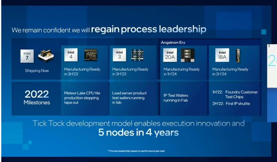
When laying out its upcoming foundry nodes following the current Intel 7 (10 nm enhanced SuperFin), the company mentioned its successors, starting with Intel 4 (7 nm EUV-based), which offers electrical properties and transistor densities in the league of 5 nm-class nodes by TSMC. Intel 4 debuts with "Meteor Lake" mobile architecture slated for the first half of 2023, with mass-production of wafers commencing in 2H-2022. The Intel 3 node is targeted for a year later in late-2023, with the server processor that succeeds "Sapphire Rapids" being developed for this node. Following this, Intel, along with several other foundry companies, enter the tricky sub-2 nm class.
The Intel 20A (20-angstrom) node is being designed for a specific category of Intel processors slated for the first half of 2024. Later that year, the company will debut the Intel 18A (18-angstrom) node. Intel unveiled the new "Arrow Lake" client microarchitecture being developed on the Intel 20A node, with product-launches expected in 2024, and wafer production in 2023. The company appears to be de-coupling its server, client desktop, client-mobile, GPU/XPU accelerators from each other, with the development of specific nodes for each. These will then be combined in some shape or form as hardware IP blocks on purpose-built multi-chip modules, such as the upcoming "Ponte Veccio."
Add your own comment

25 Comments on Intel "Tick Tock" Alive Again, Company Announces New Intel 18A Node (1.8 nm Class)

#1
Tom Yum
Pretty easy to start Tick Tock again when you can call a process whatever the hell you like regardless of what physical attributes it has. I know TSMC do it as well, but it does make the concept of Tick Tock as a return to form meaningless.
Posted on Reply
#2
Assimilator
Tom YumPretty easy to start Tick Tock again when you can call a process whatever the hell you like regardless of what physical attributes it has.
ArticleThe Intel 20A (20-angstrom) node is being designed for a specific category of Intel processors slated for the first half of 2024. Later that year, the company will debut the Intel 18A (18-angstrom) node.
Reading comprehension much?
Posted on Reply
#3
punani
Tom YumPretty easy to start Tick Tock again when you can call a process whatever the hell you like regardless of what physical attributes it has. I know TSMC do it as well, but it does make the concept of Tick Tock as a return to form meaningless.
naah only if they would ever re-name the same fabrication process it would be useless.. "back to tick tock" is because they in recent times had a process shrink every third generation.
Posted on Reply
#4
TheoneandonlyMrK
AssimilatorReading comprehension much?
What's there to read , no size spec for 20A quoted and no details for the size of 18A means they are that, because we said so.

They're leap frogging bullshit (tsmc node sizes) by doubling the bullshit , not halving the size.
Posted on Reply
#5
catulitechup
fancy and cheap names like pat

but new slides dont be new products now, intel king of future paper products

:)
Posted on Reply
#6
phanbuey
Yes! they totally suck... Please keep selling their stock.
Posted on Reply
#7
r9
Slide making department seems to be working with full steam.
Posted on Reply
#8
Vayra86
Bwahhahaahahahha


/thread

PS. Pat stinks like old socks. Still does.
Posted on Reply
#9
Cutechri
Wake me up when Nova Lake arrives.
Posted on Reply
#10
R-T-B
TheoneandonlyMrKWhat's there to read , no size spec for 20A quoted and no details for the size of 18A means they are that, because we said so.

They're leap frogging bullshit (tsmc node sizes) by doubling the bullshit , not halving the size.
en.m.wikipedia.org/wiki/Angstrom
Posted on Reply
#12
trsttte
TheoneandonlyMrKAre pulling my leg ,I know what a Angstrom is I'm an engineer , I don't know what intel's nodes have To Do with them besides a name though.
It's the next step after nanometers (i mean it's still nanometers but 1.8nm probably sounded weird lol). It's meaning, besides being just a name, is the same as intel 7 or 10nm or Tsmc 7nm or whatever. Node names departed any meaning long ago so Intel was like "we're getting killed by marketing, fuck it, let's do it as well"
Posted on Reply
#14
TheoneandonlyMrK
trsttteIt's the next step after nanometers (i mean it's still nanometers but 1.8nm probably sounded weird lol). It's meaning, besides being just a name, is the same as intel 7 or 10nm or Tsmc 7nm or whatever. Node names departed any meaning long ago so Intel was like "we're getting killed by marketing, fuck it, let's do it as well"
It's total horse shit from Intel's, Tsmc's or anyone else's mouth , IMHO unless it's real.

When they're actually at 20Angstrom features the performance will make a chip with "Characteristics of 20A total binable rubbish.
Posted on Reply
#15
R-T-B
TheoneandonlyMrKAre you pulling my leg ,I know what a Angstrom is I'm an engineer , I don't know what intel's nodes have To Do with them besides a name though.
I didn't know you were an engineer, sorry. Job titles don't autotransmit online. Just making sure you knew the unit.

I know there's no way it's truly 20A but just thought the unit educational material.
Posted on Reply
#16
mechtech
“Intel, along with several other foundry companies, enter the tricky sub-2 nm class.”

I was hoping for sub-14nm class for humour ;)
Posted on Reply
#17
Vayra86
WirkoSemiAccurate had a nice write-up about that. Intel followed the advice and didn't rename the nodes; yet, at the same time, they did rename the nodes.
www.semiaccurate.com/2021/04/07/intel-should-not-rename-their-processes/
Exactly.

Note this:
"A good example of this is Nvidia’s current GeForce 3000 line of GPUs. A few of the high end parts are made on TSMC 7nm and several others are made at Samsung. On what node? 8nm. That is basically 7nm so all good, right? As we mentioned SS7 is effectively AWOL, 8nm is a 10nm derivative made to look like it was close to 7nm. Unfortunately the performance characteristics give it away as we went in to a bit here."
Posted on Reply
#19
ModEl4
My understanding was that we would have Meteor Lake on 4nm, Arrow Lake on 3nm and then Lunar Lake on 20A and finally Nova Lake on 18A,
www.techpowerup.com/img/BfbZJotajpiM4woY.jpg
but seeing the below slide confused me (18A for Lunar):
cdn.videocardz.com/1/2022/02/Arrow-Lake-Lunar-Lake.jpg
Even more confusing is that it suggests that 2023 Meteor Lake will have 4nm compute, 20A AI and TSMC 3nm graphics tiles, is 20A going to be ready for 2023 mass launch? (even if it is only for small AI compute tiles)
Posted on Reply
#20
R-T-B
AssimilatorPeople are still using SemiAccurate as a "news" source in 2022?
I mean it is the era of "fake-news" so...
Posted on Reply
#21
ghazi
trsttteIt's the next step after nanometers (i mean it's still nanometers but 1.8nm probably sounded weird lol). It's meaning, besides being just a name, is the same as intel 7 or 10nm or Tsmc 7nm or whatever. Node names departed any meaning long ago so Intel was like "we're getting killed by marketing, fuck it, let's do it as well"
Intel can't really complain given they started it by calling their 26nm node "22nm".
Posted on Reply
#22
R-T-B
ghaziIntel can't really complain given they started it by calling their 26nm node "22nm".
Didn't FinFET and other advances make straight node measurements as names misleading in their own right though?

There really isn't a straight answer to the problem. It's complicated, is the bottom line.
Posted on Reply
#23
ghazi
R-T-BDidn't FinFET and other advances make straight node measurements as names misleading in their own right though?

There really isn't a straight answer to the problem. It's complicated, is the bottom line.
Sure, especially relative to planar nodes, that was the whole justification behind calling it "22nm", though if I'm not mistaken the fabs always targeted whatever the ITRS said would be the "next gen node" size anyway. But that's what set the precedent for every fab making up the names of their nodes out of thin air. And of course it's been complicated for even longer than that, the "minimum feature size" already didn't mean all that much and gate length was decoupled from the advertised node size many years ago, but at least it was a tangible quantity that had some relation to reality. Now we mostly just have these theoretical SRAM cell densities to go off of and looking at transistor counts of actual products where density on the same node can vary by a factor of >1.6, and we also know well enough that density doesn't translate to performance anymore. It's a big mess for marketers to deal with, but nonetheless that is the origin point of node nomenclature having no meaning. If Intel can just arbitrarily declare its physical 26nm node is "equivalent" to a 22nm node using old transistor tech then anyone else can do the same to get one up over the competition.
Posted on Reply
#24
jimmyxxx
The limit of transistor shrinking is the Silicon atom size, which is about 0.2nm. Realistically and with the current technology we can get to about 1nm in size, because there needs to be a big enough gap for electrons to jump in a controlled way, smaller gaps allow electrons to sporadically jump without any input. Smaller transistors require new semiconductor materials with a smaller atom size, or with better properties that allow the gap to be even smaller. Another way would be inventing a transistor that doesn't use the Field Effect to perform its duties.
Posted on Reply
#25
Prima.Vera
This is all good news, however they never mention the yields percentage.
Are those going to be horrid, just like Samsung's 5nm and 4nm ones (~35%), or even lower...?
Posted on Reply
Add your own comment
Apr 25th, 2024 19:38 EDT change timezone

New Forum Posts

Popular Reviews

Controversial News Posts