Wednesday, February 14th 2024

Intel Core i9-14900KS Draws as much as 409W at Stock Speeds with Power Limits Unlocked

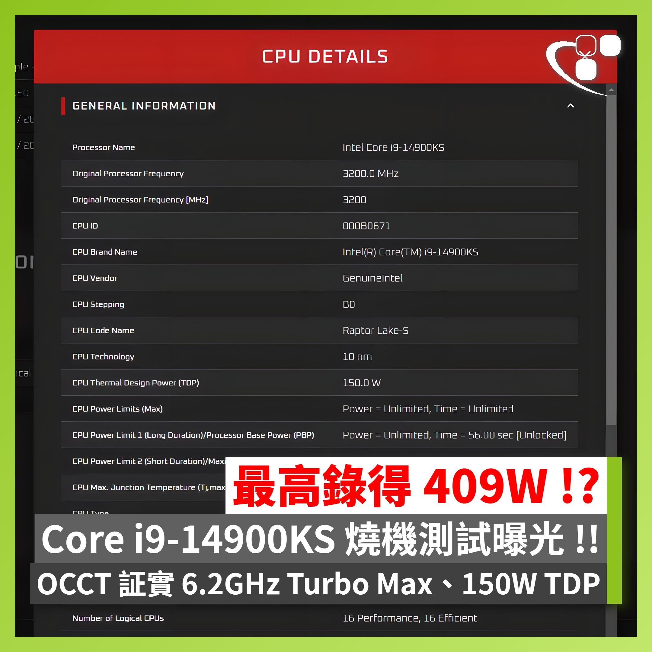
Intel's upcoming limited edition desktop processor for overclockers and enthusiasts, the Core i9-14900KS, comes with a gargantuan 409 W maximum package power draw at stock speeds with its PL2 power limit unlocked, reports HKEPC, based on an OCCT database result. This was measured under OCCT stress, with all CPU cores saturated, and the PL2 (maximum turbo power) limited set to unlimited/4096 W in the BIOS. The chip allows 56 seconds of maximum turbo power at a stretch, which was measured at 409 W.

The i9-14900KS is a speed-bump over its predecessor, the i9-13900KS. It comes with a maximum P-core boost frequency of 6.20 GHz, which is 200 MHz higher; and a maximum E-core boost frequency of 4.50 GHz, which is a 100 MHz increase over both the i9-13900KS and the mass market i9-14900K. The i9-14900KS comes with a base power value of 150 W, which is the guaranteed minimum amount of power the processor can draw under load (the idle power is much lower). There's no word on when Intel plans to make the i9-14900KS available, it was earlier expected to go on sale in January, along the sidelines of CES.
Source: HKEPC
Add your own comment

228 Comments on Intel Core i9-14900KS Draws as much as 409W at Stock Speeds with Power Limits Unlocked

#126
AusWolf
lexluthermiesterIn all fairness, the highend market drives a lot of sales and always has. I love these kinds of models because I can appear to the folks with the money to burn and offer them the best of the best.
Well, if you do that for a living, fair enough. :) I just give tips to friends and colleagues, and I always tell them to stay away from these money pits.
Posted on Reply
#127
londiste
So, as pointed out elsewhere, in addition to Default Power Profile at 253W the 13900KS has the Extreme Power Profile at 320W that motherboard manufacturers will mostly default to. So that is what the stock in case of 14900KS will likely mean. Yes, unreasonably high, but the initial headline and claim is still bullshit.
Posted on Reply
#128
AusWolf
londisteSo, as pointed out elsewhere, in addition to Default Power Profile at 253W the 13900KS has the Extreme Power Profile at 320W that motherboard manufacturers will mostly default to. So that is what the stock in case of 14900KS will likely mean. Yes, unreasonably high, but the initial headline and claim is still bullshit.
The headline says "with power limits unlocked", and not "by default".
Posted on Reply
#129
londiste
AusWolfThe headline says "with power limits unlocked", and not "by default".
It also says "stock".
Judging by comments in the thread this is what most people seem to have as the main takeaway.
Posted on Reply
#130
bug
pavleThat is a good question. If you look at power tests, maximum power for it seems to suggest that and it's always better to honestly tell the max. value than intel's average usage numbers so one can choose the proper cooling system.
The real problem is people don't understand TDP (or modern CPUs).
A quick look at Wikipedia can clear things up rather quickly: TDP means "Thermal Design Power" or "Thermal Design Point". It's the amount that needs to be handled by the solution design (the second definition is better imho, since it points out (pun) it's just a point).
Sure, this means CPU reviews don't always look at CPUs running (constrained) at their rated TDP, so if you're looking at the numbers for a 14100 running on a platform that is built for a 14900KS, you will see some numbers that you won't necessarily see in your own system. But that's a flaw* in the review procedure, not in the CPU itself or the numbers on the box.

*most reviewers will use one system for all CPU reviews, to offer an apples-to-apples comparison. Not everybody has the time to run TDP constrained tests. But TPU does, even if they don't do it for every single CPU.
Posted on Reply
#131
BoggledBeagle
Dr. DroSee this for reference:

Where is this picture from? You have 60% of the Die quality axis occupied with chips with all 24 cores fully functioning, which is obviously wrong.

In each case, 14900KS will be probably pretty rare.
Posted on Reply
#132
Chrispy_
Have any sites done a power efficiency scaling article on 14th-gen yet?

12th-gen was the last time I saw such articles and the result of those was that Alder Lake performed decently at 200W with very little benefit to uncapping the power limits (~350W power draw)

I'm just curious how well 14th-gen scales at PL1+PL2 power limits ranging from 65W to 409W. I'm willing to bet that the performance/Watt curve flattens off considerably beyond 175W or so and that everything beyond that is akin to just throwing hundreds of Watts away for single-digit percentile gains. Let's face it, if it can clock to 5.4GHz at 125W, is it really worth throwing 227% more power at it for 10% faster clocks, resulting in probably 7-8% more performance?
Posted on Reply
#134
Chrispy_
BoggledBeagleWhere is this picture from? You have 60% of the Die quality axis occupied with chips with all 24 cores fully functioning, which is obviously wrong.

In each case, 14900KS will be probably pretty rare.
Indeed, Intel are pretty tight-lipped about their yields outside of overly-optimistic investor-baiting presentations, and even then - expecting more than about 50% of all dies to have totally flawless P-cores, cache, IGPs, and three flawless e-core clusters is probably unrealistic. If their yields were this good they'd be shouting it from the rooftops.

This is what I think is more accurate (adjusted by me, obvs...)

BoggledBeagleArticles and forum posts about performance of power limited 13th and 14th gen CPUs are plentiful.

For example:

www.techpowerup.com/review/intel-core-i9-14900k-raptor-lake-tested-at-power-limits-down-to-35-w/

more to follow
Thanks, that only really covers undervolting though as all results are 253W PL2 only or lower.

I can't remember where I saw it but somewhere plotted results out like this, all the way to 350W or so:
Posted on Reply
#135
BoggledBeagle
Chrispy_I can't remember where I saw it but somewhere plotted results out like this, all the way to 350W or so:
It could have been my graph from Anandtech forum, I got an early 13900K sample and published some power limit efficiency tests there. I am at work, so I do not have access to my computer and I am also banned on Anandtech forum, so I cannot download pictures from there. I only had the above table in my work computer by chance.
Posted on Reply
#136
Chrispy_
BoggledBeagleIt could have been my graph from Anandtech forum, I got an early 13900K sample and published some power limit efficiency tests there. I am at work, so I do not have access to my computer and I am also banned on Anandtech forum, so I cannot download pictures from there. I only had the above table in my work computer by chance.
It was a first-party, massive HW testing channel/site with a lot of results across a lot of different configs. I've searched TPU, GamersNexus, Techspot, Anand, DigitalFoundry, LTT, Hardware Unboxed, Guru3d - can't seem to find it, but it's also 12th gen, so I'm pretty sure its out of date anyway.
Posted on Reply
#137
dalekdukesboy
closeI'm getting P4 EE vibes.
Oh the good old days. I still have a p4 motherboard in a box in my attic circa turn of the century lol.
Posted on Reply
#138
A Computer Guy
Vya DomusThose security issues wont go away if you disable SMT.
Sorry I meant to say HT.
Posted on Reply
#139
Onasi
Honestly, I respect the people who would buy this. They know it makes 0 sense in any way, they just want a Bugatti Chiron as a daily driver. It’s fairly silly, but I respect the commitment to the ostentatiousness. For everyone else there are saner products for any usecase and at any price tier.
Posted on Reply
#140
AnotherReader
lexluthermiesterIf by SMT you mean Symmetric-Multi-Tasking, then no they didn't get rid of it. If I understand correctly(and I admit I might not), they simply changed the way it was implemented without changing the effective functionality.
I'm referring to simultaneous multithreading. This is all based on rumours so we can't be sure about the details, but these rumours indicate that SMT is missing from the cores. Now the leaks don't say whether it's disabled or missing from the design altogether. The ability to multi-task, of course, is separate and has a far more primitive ancestor for x86 CPUs: the 80286.
Chrispy_Indeed, Intel are pretty tight-lipped about their yields outside of overly-optimistic investor-baiting presentations, and even then - expecting more than about 50% of all dies to have totally flawless P-cores, cache, IGPs, and three flawless e-core clusters is probably unrealistic. If their yields were this good they'd be shouting it from the rooftops.

This is what I think is more accurate (adjusted by me, obvs...)


Thanks, that only really covers undervolting though as all results are 253W PL2 only or lower.

I can't remember where I saw it but somewhere plotted results out like this, all the way to 350W or so:
As far as yields are concerned, we would need to know the defect rate and then we could calculate a lower bound on it using one of the chip yield calculators. The 13900k has a die size of 257 mm^2. If there defect density is similar to TSMC's N7 from Q3 2019, shortly after the introduction of Zen 2, then the yield for even this large die would be about 80%. Now we have no way of knowing what their yields are, but given their troubles, I would expect them to be closer to TSMC's troubled 40 nm node. A defect density of 0.4 per square cm would mean only 39% of dies qualifying as fully functional while 0.3 would improve that to 49%.
Posted on Reply
#141
Dr. Dro
BoggledBeagleWhere is this picture from? You have 60% of the Die quality axis occupied with chips with all 24 cores fully functioning, which is obviously wrong.

In each case, 14900KS will be probably pretty rare.
I think I had it saved from either here on TPU or a thread on Twitter but I don't think it's that wrong. The 14700K kind of proves that, they're on average similar to the 13900K and Intel's been disabling an e-core cluster just because. Yields on Intel 7 are excellent at this point because the node is very mature.
Posted on Reply
#142
Chrispy_
AnotherReaderAs far as yields are concerned, we would need to know the defect rate and then we could calculate a lower bound on it using one of the chip yield calculators. The 13900k has a die size of 257 mm^2. If there defect density is similar to TSMC's N7 from Q3 2019, shortly after the introduction of Zen 2, then the yield for even this large die would be about 80%. Now we have no way of knowing what their yields are, but given their troubles, I would expect them to be closer to TSMC's troubled 40 nm node. A defect density of 0.4 per square cm would mean only 39% of dies qualifying as fully functional while 0.3 would improve that to 49%.
Indeed, hard to know because Intel don't really publish their yield results (they don't have to sell their process node to other people so there's no need to boast about the yields) but we know that Intel 10++, aka Intel 7 has had a very rough journey indeed. It's obviously salvageable at this point but I don't think anyone in the silicon industry would call it a good node.

I presume you're plugging your estimates into a wafer yield calc like this, right?
cloud.mooreelite.com/tools/die-yield-calculator/index.html
Posted on Reply
#143
CyberCT
LOL! As I glare down at the 24w APU power consumption on my ROG Ally, playing almost all games at great frame rates.

I have two desktops running 11900ks, but I clock limited them to 4.8ghz and undervolted them. Learned quickly the sweet spot is ideal for almost everything and chasing an extra few frames for 100+ watts more just isnt' necessary 95% of the time.
Posted on Reply
#144
Chrispy_
Dr. DroI think I had it saved from either here on TPU or a thread on Twitter but I don't think it's that wrong. The 14700K kind of proves that, they're on average similar to the 13900K and Intel's been disabling an e-core cluster just because. Yields on Intel 7 are excellent at this point because the node is very mature.
Got a source on that?

Google says that 10 months ago Intel 7 yields were just 53% as good as TSMC 7, so they're half as good as their competitors were 5 years ago. Granted, that's not a thorough search into the topic and in fairness to Intel, TSMC 7nm yields were very good - but if the first couple of results say that Intel yields were still poor 10-11 months ago, what major development have Intel had since then that would change anything, and if so - why aren't they boasting about huge yield improvements rather than putting out the same stuff as before at higher TDPs and lower efficiencies than ever?

In general, if there is no change, there is no news and therefore no search results, which is why the top results are almost a year old.
Posted on Reply
#145
AnotherReader
Chrispy_Indeed, hard to know because Intel don't really publish their yield results (they don't have to sell their process node to other people so there's no need to boast about the yields) but we know that Intel 10++, aka Intel 7 has had a very rough journey indeed. It's obviously salvageable at this point but I don't think anyone in the silicon industry would call it a good node.

I presume you're plugging your estimates into a wafer yield calc like this, right?
cloud.mooreelite.com/tools/die-yield-calculator/index.html
You're right; getting numbers for TSMC is far easier because they are courting clients and showcasing their progress to investors. However, there have been instances of broken nodes in the past that worked fine in the end; TSMC's 40 nm comes to mind. However, Intel 7 has had a far rougher time than any node I can recall so its yields might still not be good enough even by that low bar. That 40 nm process had a defect density of 0.3 to 0.4 around the time the Radeon 5870 launched, but AMD was able to work around it; Nvidia, on the other hand, had troubles launching Fermi until TSMC got the process sorted out. Yes, I'm using one of the online calculators, e.g. this one by iSine.
Posted on Reply
#146
Dr. Dro
Chrispy_Got a source on that?

Google says that 10 months ago Intel 7 yields were just 53% as good as TSMC 7, so they're half as good as their competitors were 5 years ago. Granted, that's not a thorough search into the topic and in fairness to Intel, TSMC 7nm yields were very good - but if the first couple of results say that Intel yields were still poor 10-11 months ago, what major development have Intel had since then that would change anything, and if so - why aren't they boasting about huge yield improvements rather than putting out the same stuff as before at higher TDPs and lower efficiencies than ever?

In general, if there is no change, there is no news and therefore no search results, which is why the top results are almost a year old.
It's more guesswork than anything I must confess, the fact that they're mass producing chips like the 14900K at this point proooobably mean that the yields are just fine. After all, they've been making these CPUs on the same node for three years by now.
Posted on Reply
#147
AnotherReader
Dr. DroIt's more guesswork than anything I must confess, the fact that they're mass producing chips like the 14900K at this point proooobably mean that the yields are just fine. After all, they've been making these CPUs on the same node for three years by now.
Increasing die sizes of higher volume products like laptop SKUs and some desktop SKUs are likely to be an indicator of improving yields. Die sizes have increased as the process has matured. Cannon Lake, which Intel has almost disowned, is 70.5 mm^2 while Tiger Lake, the first decent Intel 7 product, is more than twice as large at 146.1 mm^2. Raptor Lake has pushed this all the way up to 257 mm^2 which is a very large die for desktops. In recent times, only Bulldozer and Istanbul, the 6 core Phenom II die, had significantly larger dies at 315 and 346 mm square respectively.
Posted on Reply
#148
marios15
Yields are at least 80-85% for the full die, otherwise they wouldnt be releasing CPUs near 6GHz
Posted on Reply
#149
AnotherReader
marios15Yields are at least 80-85% for the full die, otherwise they wouldnt be releasing CPUs near 6GHz
You are conflating parametric yield loss and catastrophic yield loss (link to PDF). However, Intel also sells an enormous 770 mm^2 die: the monolithic variant of Sapphire Rapids. Given that this is sold for servers, they wouldn't need very high yields for it to make sense. Still, defect density can't be too bad or they would hardly get any functional dies out. A defect density of 0.4 per cm^2 would result in just 9.6% of the Sapphire Rapids-MCC dies being fully functional.
Posted on Reply
#150
wNotyarD
londisteIt also says "stock".
Judging by comments in the thread this is what most people seem to have as the main takeaway.
It also says "speeds". Unlocking power while keeping speeds at stock isn't impossible, you know?
Posted on Reply
Add your own comment
May 13th, 2024 16:11 EDT change timezone

New Forum Posts

Popular Reviews

Controversial News Posts