Friday, May 24th 2024

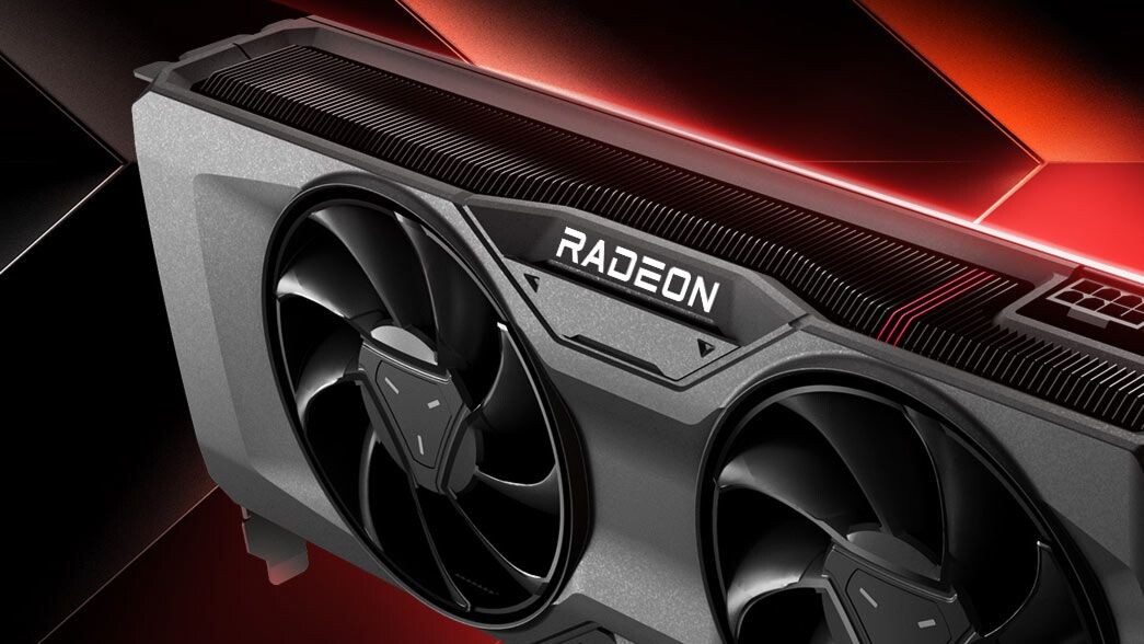
AMD Adds RDNA 4 Generation Navi 44 and MI300X1 GPUs to ROCm Software
AMD has quietly added some interesting codenames to its ROCm hardware support list. The biggest surprise is the appearance of "RDNA 4" and "Navi 44" codenames, hinting at a potential successor to the current RDNA 3 GPU architecture powering AMD's Radeon RX 7000 series graphics cards. The upcoming Radeon RX 8000 series could see Navi 44 SKU with a codename "gfx1200". While details are scarce, the inclusion of RDNA 4 and Navi 44 in the ROCm list suggests AMD is working on a new GPU microarchitecture that could bring significant performance and efficiency gains. While RDNA 4 may be destined for future Radeon gaming GPUs, in the data center GPU compute market, AMD is preparing a CDNA 4 based successors to the MI300 series. However, it appears that we haven't seen all the MI300 variants first. Equally intriguing is the "MI300X1" codename, which appears to reference an upcoming AI-focused accelerator from AMD.
While we wait for more information, we can't decipher whether the Navi 44 GPU SKU is for the high-end or low-end segment. If previous generations are for reference, then the Navi 44 SKU would target the low end of the GPU performance spectrum. The previous generation RDNA 3 had Navi 33 as an entry-level model, whereas the RDNA 2 had a Navi 24 SKU for entry-level GPUs. We have reported on RDNA 4 merely being a "bug correction" generation to fix the perf/Watt curve and offer better efficiency overall. What happens finally, we have to wait and see. AMD could announce more details in its upcoming Computex keynote.
Sources:
Kepler_L2, via Tom's Hardware
While we wait for more information, we can't decipher whether the Navi 44 GPU SKU is for the high-end or low-end segment. If previous generations are for reference, then the Navi 44 SKU would target the low end of the GPU performance spectrum. The previous generation RDNA 3 had Navi 33 as an entry-level model, whereas the RDNA 2 had a Navi 24 SKU for entry-level GPUs. We have reported on RDNA 4 merely being a "bug correction" generation to fix the perf/Watt curve and offer better efficiency overall. What happens finally, we have to wait and see. AMD could announce more details in its upcoming Computex keynote.
22 Comments on AMD Adds RDNA 4 Generation Navi 44 and MI300X1 GPUs to ROCm Software
But that aside, if RDNA 4 is any good, which means power efficient enough and neat specs, I would still consider upgrading from my 6600 XT.
I was wondering if that was the number of ASICs dedicated to RT, but it doesn't make sense either, if one is a successor to the RX 7600, the gap in "RT core count" wouldn't be that great.
Edit: I found a good summation of everything RDNA4. The article places the Navi 48 ahead of the Navi 44 but claims 64 CUs instead of my estimate of 80 CUs. Here is the performance prediction:
"Comparing the flagship RDNA 4 card to the rest of the competition tells a different story. Most sources estimate that the rumored RX 8800 XT should be close to the RX 7900 XT in performance. Moore’s Law Is Dead says that it’ll be around 10% slower than the RX 7900 XTX, putting it close to Navi 31 and Nvidia’s RTX 4080. It should outperform the RTX 4070 Ti Super by a small margin, and RedGamingTech predicts that it’ll be slightly faster than the recent RX 7900 GRE."
AMD RDNA 4: Everything we know about the RX 8000 series | Digital Trends
64 CUs, 80 CUs, either way, predictions are saying 7900 level performance.
This is so true that AMD found itself with room(It's still 4nm) to add dedicated RT ASICs and perhaps even AI-related paraphernalia.
Examining AMD’s RDNA 4 Changes in LLVM – Chips and Cheese
AMD RDNA 4: Everything we know about the RX 8000 series | Digital Trends
TSMC Details N4X Process for HPC: Extreme Performance at Minimum Leakage (anandtech.com)
N4P brings +8-11% (depending on which company you ask) clocks. N4X another 3-4% on top of that.
I've long looked to the A16/M2 for guidance on what to expect; Snapdragon is similar (3.2-3.4 mobile, 3.8 SDX). It may be lower, but I still think 3.2-3.4ghz stock is likely, with at least 3.5ghz OC; maybe higher.
Do we even know for certain it's N4P? Perhaps that's true, but when I see something like the N4X process even existing...I instantly think of RV790. 55HP was a partnership with TSMC for (only?) that chip.
A thing to note about RV790 (vs RV770) was, and I quote: "AMD revised the core by adding decoupling capacitors, new timing algorithms, and altered the ASIC power distribution for enhanced operation".
Hmm. Yep, that pretty much sounds like what they need to do (AFAICT).
I can't think of many companies that would desire, let-alone use a "X" process, which is about clocks (and perhaps conserving die size vs a larger unit design), not power savings. Certainly not Apple; likely not nVIDIA.
As I mentioned in another thread, it's existance reminds of nothing other than that particular instance, and really is the lineage of chips dating back to RV670 (which launched one year after AMD acquired ATi).
That has been and continues to be my prediction/speculation, but some or all of it could be wrong.
Assuming they enhanced (perhaps 4-bit, but) 8-bit operations (AI/RT), would you not consider that a high-end chip (If, say, if it could [even overclocked] average 1440p120 mins across TPU's suite...just like a 4080)?
Similarly, I think the opportunity is there not only to absolutely destroy the 4060 Ti(/S?) 16GB in value, but compete with (XSX/PS5 vanilla) consoles w/ higher perf for less money; maybe similar dosh to a XSS.
Also, it's interesting AMD's market-share generally goes up when they release value-oriented products (RX480, 5700xt, 6600/6700/6800-series price-drops when 6650/6750/6950xt launched; ~$200-600).
Wrt consumers though, it could actually be a logical tipping point back to PC (as generally happens around this point in the cycle; perhaps this time nVIDIA be-damned) if you ONLY need a GPU upgrade.
Why buy a (7800xt-like) PS5 pro if there is a similar-priced 4080 competitor? Why buy a PS5/XSX if there is a faster product for cheaper? Why buy a XSS if there is a XSX-level card for a similar price?
I suppose it's foolish to go so hard into speculation when the reality isn't far away, but it's what I would do...while there doesn't appear to be evidence against it.
Not only is it feasible, it's the only two markets that are really important (wrt volume). I understand that margins are key (that's why people like nVIDIA, right?), but wrt AMD, they need mindshare/market-share uptake.
I can't think of a better way to do that create and sell parts that are tangibly-better than console options for a similar price, or sometimes lower, depending upon the comparison.
That said, I don't see why they would use more than 8192sp. Even if AI/RT scales linearly with RDNA2, that's still 128 AI Engines and 64 RT accelerators.
They trail nVIDIA by what, ~20% clock-per-clock in RT (I forget)? You can see why would want to boost the units slightly (even with a clockspeed bump), else they would require a clockspeed of 3300mhz to even compete with GA104. That's simply not good-enough; they have to beat GA104 (old 4070 Ti) regardless of how well clockspeeds turn out, and this affords them a couple hundred mhz leeway.
Also, in the past, the golden ratio to 64 ROPs would've been something like 7511-7512 units. While 7800xt already has 96 ROPs, it makes sense to add the units because of space afforded by 4nm, especially if they are able to do that and still ramp the clockspeed to it's greatest potential within 375w.
This is just speculation on my part, but I have to wonder if the N41/N42/N43 'designs' were based on N4C configurations; perhaps refreshes/shrinks were (internally) N45/46/47.
When they decided to shift that whole chiplet design to RDNA5, I wonder if the monolithic chips they replaced them with inevitably became N44 and N48 simply as they went into design much later.
It's kind of like how we had R300 (9700)->R420 (x800). Why was there no R400? Because it got scrapped for being kinda-sorta in a similar situation to N4C (although it did go into the Xbox 360).
Also why is RV530 slower than R520? Because the refreshed arch was newer and the new R520 was R580. Same holds true for then going to R670 for the higher-end and lower-numbers for the lower-end.
Of course, then we got trees, islands, and all that stuff.
I'm sure there's some rhyme or reason to do it, but it's not like AMD hasn't changed up their internal naming schemes numerous times in the past.
One can only assume it's because the original versions that followed the previous convention were scrapped, as that's what has happened before, but I can't speak for certain.
Hopefully some day the complete story will come to be told, as those are usually pretty interesting, imo.
Navi 33 7600
Navi 32 7800
Navi 31 7900
Also the numbers are no longer 1,2,3.
Navi 48 8700/8800
Navi 44 8500/8600
A design aimed at competing in the most sensitive market in terms of performance/price(Mid/Low-end) has to be lean and extract every % of performance from the silicon possible.
64CU in more efficient architecture at higher frequency can be easily equivalent to or faster than 80CU RDNA3. We are talking about a gap of only 25%.
Navi 48: 32 WGP + 48MB of Infinity Cache + GDDR7 memory + 192-bit memory bus + PCIe 5.0 x16
Navi 44: 20 WGP + 32MB of Infinity Cache + GDDR7 memory + 128-bit memory bus + PCIe 5.0 x8
or
Navi 48: 32 WGP + 32MB of Infinity Cache + GDDR7 memory + 128-bit memory bus + PCIe 5.0 x8
Navi 44: 20 WGP + 24MB of Infinity Cache + GDDR7 memory + 96-bit memory bus + PCIe 5.0 x8
www.tweaktown.com/news/94533/amds-next-gen-rdna-4-navi-44-and-48-from-radeon-rx-8000-series-gpus-appear-in-linux/index.html
It is literally the benchmark for $ people will pay in that segment, hence you've seen it drastically fluctuate in price over time.
People forget 7800xt runs at 2425mhz stock. While W1zard showed 2551, most report 2448mhz for 7900xt. We've seen 7900xtx [2631 avg wrt W1z] at 3200mhz (and someone recently froze it for 3390mhz) OC.
This is closer to what the arch was intended, imho, but it was and/or AMD held it back for whatever reason (probably power/heat/yield/price).
The jumps (on the stock charts) will appear huge to the avg Joe because RDNA3 ran at very low clocks (and even 7900gre was limited wrt overclocking not only through PL, but actual bios-limiting of clocks).
To people that overclocked the 7800xt/7900xt to ~2900mhz, these lifts will not look as substantial, but it still matters because of relative performance to 4080, and price/perf to 4070 Super/4070 Ti Super.
The same will (prob) be true of N44/4060 Ti 16GB (XSX): where-as 7600 was just about getting perf similar to a PS5; for PC gamers to keep up with relevant gaming on standard console platforms for cheap.
The efficiency yield/curve (of 5nm) appeared to be around 2900mhz. You see this not only is around the stock clock of Ada (~2730mhz), but it's overclock potential. It sits fairly perfectly on the curve.
The point of RDNA3 was to maximize clock potential with less silicon (over the perf/w curve), but for w/e reason that didn't work (wrt power/[heat?] efficiency) and/or was held back in certain circumstances.
I would imagine RDNA4 not only fixes this, but also adds the performance additions of 4nm (P or X).
You also have to remember the density of non-logic xtors on (5nm) would shrink to .021 from .027 on 7nm.
Yes, they (the MCDs) were 6nm and this is 4nm, but remember that even 3nn only shrinks non-logic/sram xtors to .0199 (and it increases on n3e back to 5nm level).
While I have no idea how sram size was effected on 6nm (from 7nm) and/or how it is on 4nm (from 5nm), it's likely by incorporating it on-chip *may* make it just about as small as it can get (similar to N3B).
This is important, because (as shown with RDNA2) AMD truly does need that extra cache; it would make sense if L3/IC were doubled from 32/64 to 64/128MB, but ofc there are other ways to go about it too.
If you look at a MCD, or even v-cache on their CPUs, 16MB of cache is not very large...so it makes sense, especially when compared to perhaps expensive/less power-efficient 24gbps GDDR6 to increase bw.
I find it interesting when people mention it could use 18gbps GDDR6. While supporting the idea of the larger cache and cheapest memory (making the product sustainable wrt bw but also cheap), IDK about 18gbps.
This is because Samsung literally EOL'ed 18gbps RAM, and Hynix 20gbps is abundant.
I understand most use Hynix, but it would still be weird to cut out a whole supplier. I think sustaining 20Gbps makes the most sense.
If it clocks well, it's possible we may see a (refresh/later) iteration with 24gbps from Samsung. It's unknown at this time if it will require that (given likely cache improvements), but it likely could utilize 20gbps regardless, which again they could dual-source and hence makes more sense. 18Gbps only makes sense if it doesn't clock as well (as I hope), cache improvements are beyond what I anticipate, or they/AIBs struck one hell of a deal with Hynix for 18gbps chips, which appears to not be the case given even low-end and/or stock products with <20gbps stock clockspeeds in-fact use 20Gbps-rated chips.
TLDR: RDNA3 was partly fubar, but was also held-back/positioned VERY OBVIOUSLY at stock to be replaced by a refresh (by both atypically low stock core/memory clocks and power/bios limitations).
RDNA4 should allow the architecture to breathe and live it's best life; hopefully scaling better with voltage/power and more evenly-spread heat, with sustainable bandwidth to perform the best it can.
But also, you know, be cheap, while performing as well as it needs to in order to pacify the required performance per segment (in theory).That is very old/third-hand (or worse) information. I respect Paul, and sometimes he is fed good information, but also sometimes he isn't. Also, things can change in development (as mentioned earlier).
That isn't his fault; he certainly *tries* to get info where he can (which is appreciated), and can sometimes be very much in the forefront of getting certain particulars of future products to the public.
That said, I don't think that information is correct.
I think you must prepare for a flop, rather than an RX 7900 level of performance.
It's why Ada doesn't really scale over ~1.07v; likely saved them area. They sacrified clockspeed potential, but likely gained power savings.
It's likely why Ada is efficient and AMD with higher clock potential is leaky at higher clocks. nVIDIA literally has a gigantic supercomputer that they use to optimize configurations and libraries on a process.
This is why you hear them complain so much when a process isn't perfect (Fermi; 40nm vias) or now even Samsung's HBM. It's because they have everything figured out down to the smallest detail.
Wrt AMD, I think they often use something closer to the more 'generic' version of a process, simply due to engineering budget.
N4P/X is an actual improvement to the inherent process, and hasn't been used in a GPU yet (afaik).
Goddamn it, I get so pissed at how successful nVIDIA is with marketing; Huang truly is like Jobs, and nVIDIA truly is like Apple. People see what they want to see/believe, and those people sell it to them.
Do not be confused; I'm not angry with you, nor do I intend to come across aggressive. You only know what you know, and you know what is marketed, but the reality is that is often bullshit.
Second, are we sure 240mm2? I know people keep saying all kinds of weird numbers, from 200-250mm or so, but I don't think this will necessarily be the case. I *could* be wrong.
I think N48 will be around the size of AD104 (counting the cache which may or may not incorporated into the main die), while N44 the size of AD106/107; somewhere around there.
I believe AMD will fight a chip one size larger from nVIDIA by using higher clockspeeds/voltage and a similar power configuration (ex: 1x8-pin, 2x-pin), but be less power-efficient..which imho doesn't matter.
It doesn't matter because the chips may reach the performance thresholds they need in order to make sense in the market (especially at their comparative price versus other options) with similar connectors.
Will [not any particular aqua-colored youtube channel] probably complain about power/heat? Probably. Will millions of people regurgitate that? Probably. Does it ACTUALLY matter to most people? No.
I'm not comparing it to 7900 levels of performance because 7900 is an extremely vague expression that creates different expectations for different people...which later people will use to bitch and complain.
It's almost-certainly a replacement for the 7900GRE...because that is where they need to compete (with the 4070 Ti Super); they need to beat it in perf...which means competing with 4070 Super in price.
That's because AMD doesn't have a Huang. Well, kinda-sorta technically they do, but let's not get into it.
But anyway, 7900GRE is a really weird SKU slapped together using all sorts of less-than-optimal configurations (like cache/bus) and (clock/power) limitations so it doesn't compete with 7900xt.
I don't think this will be. In essence, it's *potential* should be similar to that of a 7900xt (granted with less memory). It will probably be stock clocked so they can still sell 7900xt as an upgrade.
I apologize, but some people simply do not understand. Looking at W1zard's stock graphs does not tell the whole story of chips' potential or relative value. Too many people think that...and it's ignorant AF.
It's like...for example and as I've said before...some people will continue to believe a 3070 and/or Ti is a better-performing card than a 2080 Ti because of how W1zard chooses to present his charts.
Those people are fools (wrt value if they don't mind taking time to overclock). In some respects that's okay (because that might fit their use case)...I'm sure nVIDIA will sell them something with >8GB ram soon.
But, you know, it's just not true. The absolute performance of a 2080 Ti is similar to a stock 3080; and 3080 doesn't OC very well so in-fact they are very close; I'd take a 2080ti over a 3070 Ti 10/10 times....
...and the value of a 2080 Ti (at least for a long time, haven't checked lately) over a 3080 10/10 times.
The Samsung 8nm process was a POS (that nVIDIA paid very little to fab their enormous chips). The TSMC 14nm (sorry, "12nm") process was not. In some ways nVIDIA made money off of cheap logic...
...but in other ways they made it off of how they presented their newer series of chips.
nVIDIA can stock segment their cards however they want to have people perceive something as an improvement, but that doesn't make it accurate. Many times...wrt nVIDIA...and sometimes AMD...it's not.
I apologize, but I just don't feel it's likely we're going to see eye-to-eye on this. It's fine to think the way you do...but man, as an OG enthusiast...it's depressing AF that so many people think similarly.
I wish I had the time and energy to explain so many things to so many people...but it gets tiring. Too often nVIDIA often wins the market not only through marketing, but surviving the battle of attrition against them.
It is simply nvidia works more and better than AMD, who doesn't care about the graphics cards, it seems.Now I am not even sure that "4nm" exists, in the first place. WikiChip doesn't state that it exists.
Look:
en.wikichip.org/wiki/5_nm_lithography_process
en.wikipedia.org/wiki/5_nm_process
All processes are N5s.Even if it be around 300 mm^2, that doesn't mean in the slightest that Navi 48 will reach the desired clock ranges.Yeah :rolleyes:
4nm does exist.
I can't guarantee anything wrt Navi 4's ability, I was only giving a hypothesis.
I don't know if the 'yeah' is sarcastic, but it's true. The people that used to address nVIDIA's crap have largely moved on from covering it, become jaded, or have been bought off to work within the industry.