Thursday, April 9th 2026

Intel "Nova Lake-S" Uses 2L-ILM Socket for Better CPU Cooler Contact
In the latest series of leaks about Intel's upcoming "Nova Lake" chips, we learn that the desktop "Nova Lake-S" designs will feature a new socket mounting and independent loading mechanism (ILM). According to exclusive information from VideoCardz, the NVL-S desktop designs on the LGA-1954 socket will include a new 2L-ILM socket mechanism to improve contact with CPU coolers. Given that Intel's upcoming NVL-S desktop processors will have up to 52 high-frequency, power-hungry cores, a better mounting mechanism is definitely needed. This 2L-ILM is a two-level independent loading mechanism, using one lever on each side of the CPU to secure it into the LGA-1954 socket. Applying pressure on both sides of the socket ensures improved flatness while the locking mechanism does its job.
Intel categorizes its desktop sockets in various forms. One of the most basic is the Default-ILM, along with the RL-ILM. As seen with "Arrow Lake," Intel's motherboards divide the socket locking mechanism into the ILM and RL-ILM designs, applied depending on the sector. For the lower-end sector, the Default-ILM socket is used, while the RL-ILM is applied to higher-end overclocking motherboards, providing better pressure and ensuring a flatter surface contact for a cooler. Noctua and Cooler Master already differentiate these two in their CPU coolers, but the mounting hardware is generally the same for both. The RL-ILM is simply a better design for overclocking due to the improved surface contact it provides.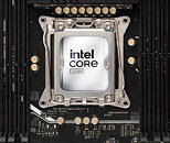 Some readers may recall that Intel used its 2L-ILM on the older LGA 2011-3 HEDT socket back in the era of X99 Express motherboards, more than a decade ago in 2014. This HEDT platform featured 2011 LGA pins, which is close to the 1954 LGA pins we see with NVL-S. It seems that having close to 2,000 pins in the LGA socket requires two levers due to the pressure needed for the application of the CPU, as the surface area needs a stronger hold to ensure that every CPU contact pin on the package is electrically touching the pins on the socket it is mounted on.
Source:
VideoCardz
Intel categorizes its desktop sockets in various forms. One of the most basic is the Default-ILM, along with the RL-ILM. As seen with "Arrow Lake," Intel's motherboards divide the socket locking mechanism into the ILM and RL-ILM designs, applied depending on the sector. For the lower-end sector, the Default-ILM socket is used, while the RL-ILM is applied to higher-end overclocking motherboards, providing better pressure and ensuring a flatter surface contact for a cooler. Noctua and Cooler Master already differentiate these two in their CPU coolers, but the mounting hardware is generally the same for both. The RL-ILM is simply a better design for overclocking due to the improved surface contact it provides.

37 Comments on Intel "Nova Lake-S" Uses 2L-ILM Socket for Better CPU Cooler Contact
I hope the mechanism has been properly designed so that if someone doesn't engage both levers simultaneously and correctly, it doesn't create uneven pressure on one side, risking bending the socket pins.
Surely one leaver on each side!
These E-cores aren't just P-cores running at lower frequencies. They are cores designed without certain features to make them more energy-efficient. Even if they were full fat P-cores running at lower frequencies, most people know how power consumption skyrockets as frequencies increase.
In any case, I would expect the text to read something like this:
'NVL-S desktop processors will feature up to 52 cores, with up to 16 of them being high-frequency, power-hungry P-cores.
With these changes, the argument is not weakened; rather, the description of the NVL-S CPUs is more accurate and avoids creating false impressions.So you are saying that because AMD fans say this and that, TPU should somehow bent the description of hybrid Intel CPUs to make them look better? You sure this is a good argument?
The only ones insisting on that example are Intel fans. Most AMD fans didn't consider those CPUs as having 'up to 8 cores.' That’s why Bulldozer CPUs were losing even to Thuban in some benchmarks. It was a bad design.
That being said, making excuses for multi-billion dollar companies that sell configurations like—to use an extreme example—1 P-core and 51 E-cores as a '52-core CPU', is not something I want to do. I guess you wouldn't have a problem with that.
I will agree that all those chocolate eggs will probably have the same sweetness and they are indeed FULL chocolate eggs.
- HEDT ILM
- HEDT-worthy number of cores
- supposedly HEDT performance
- HEDT TDP
- hopefully Celeron pricing? 🤞
Sounds about right. 🤪
Describing all 52 cores as "power hungry" shows a remarkable lack of knowledge about CPUs, and frankly should be inexcusable for a news editor of a tech forum..... There are 16 P cores, the rest are e or ultra e cores, and the efficiency of those individual cores is quite good. An efficient CPu core does not become "power hungry" because you put a dozen of them together. The PACKAGE might be "power hungry", but that is a subjective opinion, and that does not make the statement "52 power hungry cores" correct.
Those E cores are absurdly strong even on arrowlake - they're small but the density and size/count of cores puts out tons of heat.
IPC is not a measure of power consumption. And as @TheinsanegamerN said aboveNow, let's go AI. I asked Google's AI about Arrow Lake cores. We can guess more or less about Nova Lake.
So.
Power consumption under (stress test) per core
P-core (Lion Cove) 5.7 GHz ~25W+
P-core (Lion Cove) 4.6 GHz ~10W
E-core (Skymont) 4.6 GHz ~3-5W
and an estimation about the cores on Meteor/Lunar Lake I/O die
LP-E cores 0.5W - 0.8W
I've overclocked the 265K's e cores and was shocked at how much heat they could put out.
Let's suppose each P-core uses 10 W and each E-core chugs 3, you're looking at the typical 250 W TDP they're usually rated for, and that's excluding the 4 LPE that are situated on the IO tile (that's just for the 48 cores in the CPU tile). I think more realistic these CPUs can and will use 350-400 W under AVX load and high frequencies, just like RPL can do 320-350 W today.
For his bravery he was decorated with the Semiconductor Cross.1000 W tier 1 PSUs hiding in fear at the sight of the fire-breathing leviathan.
The reign of terror has begun!
Good thing I have a 1300 W unit :pimp:
@Dr. Dro
You probably haven't read the rest of the posts before posting. Everything is there for you to read.
P.S. Get ready to upgrade to 2.4KW PSU if you are considering DLSS5.
But I thought of making a little joke because of your persistence.