Wednesday, August 26th 2026

NVIDIA NVHBM Memory Promises 30% Higher Bandwidth Than HBM4E
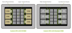
NVIDIA has announced NVHBM, a custom high-bandwidth memory technology built into the HBM base die rather than on the compute die itself. This approach, which NVIDIA plans to use in its future GPUs, is now extended to third-party XPU customers through NVLink Fusion. The main idea behind it is rather simple, since standard HBM puts the memory controller on the compute die, that is consuming silicon that could otherwise be used for compute. NVHBM moves that controller into the 3D HBM stack, which has a notable effect on performance and efficiency. Compared to standard HBM4E, NVIDIA claims up to 30% more memory bandwidth, 15% lower HBM power consumption, and up to 25% more usable compute die area on the processing unit.
The area savings come primarily from a redesigned physical memory interface. Standard HBM uses wider interface connections that increase package footprint, on the other hand, the NVHBM custom PHY reduces that I/O area by up to 67% compared to JEDEC HBM4E. Also, the narrower interface simplifies interposer routing, freeing up to 80% more usable silicon across the layout. The reduced PHY footprint also means fewer routing constraints on the interposer, which matters when you're trying to pack multiple HBM stacks alongside a large compute die, explains NVIDIA in a dedicated blog post.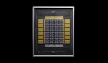
 On the power side, the 15% reduction in HBM power draw is not just about efficiency, it provides additional thermal headroom for the compute die. This matters most for enterprises and data centers where thousands of compute units operate simultaneously in hundreds of racks. NVIDIA even provided an example, in an entire 1-gigawatt data center using 2,000 W XPUs, power savings can enable up to 15,000 additional XPUs in compute headroom.
Remember that on Monday, at Hot Chips 2026, Samsung confirmed that it is preparing to ship HBM4E running at 16 Gbps per pin, up from the 14 Gbps of its current HBM4E which delivers 3.6 TB/s per stack across 2,048 pins. The step to 16 Gbps pushes that to 4 TB/s per stack. Now take into consideration that 30% NVHBM bandwidth improvement claimed by NVIDIA and a single NVHBM could theoretically hit around 5.2 TB/s.
NVIDIA says NVHBM will be validated across multiple memory vendors to simplify supplier qualification for customers and announces that Amazon's Annapurna Labs is the first confirmed partner to collaborate on NVHBM.
Sources:
NVIDIA, NVIDIA Developer Blog
The area savings come primarily from a redesigned physical memory interface. Standard HBM uses wider interface connections that increase package footprint, on the other hand, the NVHBM custom PHY reduces that I/O area by up to 67% compared to JEDEC HBM4E. Also, the narrower interface simplifies interposer routing, freeing up to 80% more usable silicon across the layout. The reduced PHY footprint also means fewer routing constraints on the interposer, which matters when you're trying to pack multiple HBM stacks alongside a large compute die, explains NVIDIA in a dedicated blog post.


Remember that on Monday, at Hot Chips 2026, Samsung confirmed that it is preparing to ship HBM4E running at 16 Gbps per pin, up from the 14 Gbps of its current HBM4E which delivers 3.6 TB/s per stack across 2,048 pins. The step to 16 Gbps pushes that to 4 TB/s per stack. Now take into consideration that 30% NVHBM bandwidth improvement claimed by NVIDIA and a single NVHBM could theoretically hit around 5.2 TB/s.
NVIDIA says NVHBM will be validated across multiple memory vendors to simplify supplier qualification for customers and announces that Amazon's Annapurna Labs is the first confirmed partner to collaborate on NVHBM.
3 Comments on NVIDIA NVHBM Memory Promises 30% Higher Bandwidth Than HBM4E
With that said, I do wonder what the PHY will look like and how much space it'll take.