Monday, September 14th 2026

Samsung and Qualcomm Forge 2.1D Packaging Alliance
Samsung and Qualcomm are reportedly forming a 2.1D Packaging Alliance to provide customers with access to advanced chip packaging using bridges that connect silicon dies. Interestingly, Samsung and Qualcomm are developing an organic bridge technology that will serve as the adhesive to hold two chips together. For example, Intel already uses a similar approach with its Embedded Multi-die Interconnect Bridge (EMIB) advanced packaging, but it employs small silicon bridges. The new 2.1D packaging alliance will use organic bridges made from materials commonly found in traditional PCBs, such as organic polymer materials like epoxy and copper wiring, to interconnect multiple chips.
This organic bridge uses redistribution layers (RDL), formed by multiple layers of fine circuitry with extremely small wires and space between them. This makes the technology more similar to PCB manufacturing than silicon manufacturing, enabling packaging densities that closely match modern silicon-based EMIB. Reportedly, Samsung will manufacture this 2.1D package using multiple RDLs packaged inside a flip-chip ball grid array package. Ultimately, the company aims for the organic bridge's line width and spacing to be 1.5 to 2 micrometers each, with via sizes of 4 to 5 micrometers. Die-to-die pattern density is targeted at 500 to 1,000 per millimeter.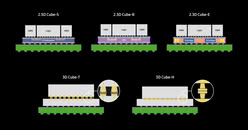 Several other customers of Samsung Foundry, alongside Qualcomm, are interested in this technology. For Qualcomm, Samsung will use this 2.1D packaging to create multi-die AI accelerators, with multiple compute dies stitched together on a single surface using this organic bridge, acting as a single unified accelerator. Qualcomm has been developing this technology for some time, as documentation points to 2024 patents for interconnect bridges. However, Samsung Foundry will be the one to manufacture this new packaging technology, as Qualcomm is a fabless chip designer.
Source:
The Elec Korea
This organic bridge uses redistribution layers (RDL), formed by multiple layers of fine circuitry with extremely small wires and space between them. This makes the technology more similar to PCB manufacturing than silicon manufacturing, enabling packaging densities that closely match modern silicon-based EMIB. Reportedly, Samsung will manufacture this 2.1D package using multiple RDLs packaged inside a flip-chip ball grid array package. Ultimately, the company aims for the organic bridge's line width and spacing to be 1.5 to 2 micrometers each, with via sizes of 4 to 5 micrometers. Die-to-die pattern density is targeted at 500 to 1,000 per millimeter.

1 Comment on Samsung and Qualcomm Forge 2.1D Packaging Alliance