News Posts matching #tile

Return to Keyword Browsing

Intel Arrow Lake-HX Interposer Appears Online

The Intel Design tools webpage has this week once again provided an early preview of upcoming processors - following on from an LGA1851-MTL-S CPU interposer appearing on the site late last month - indicating that a Meteor Lake-S desktop CPU range was due at some point later in 2023. Intel's latest webpage entry features the "BGA2114-ARL-HX Interposer for the Gen 5 VR Test Tool" with an SKU code that reads: "Q6B2114ARLHX."

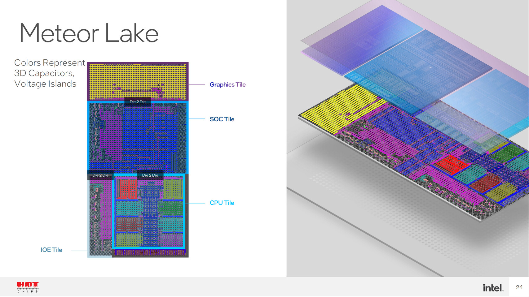
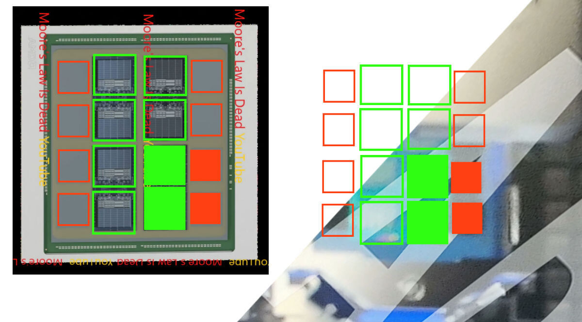
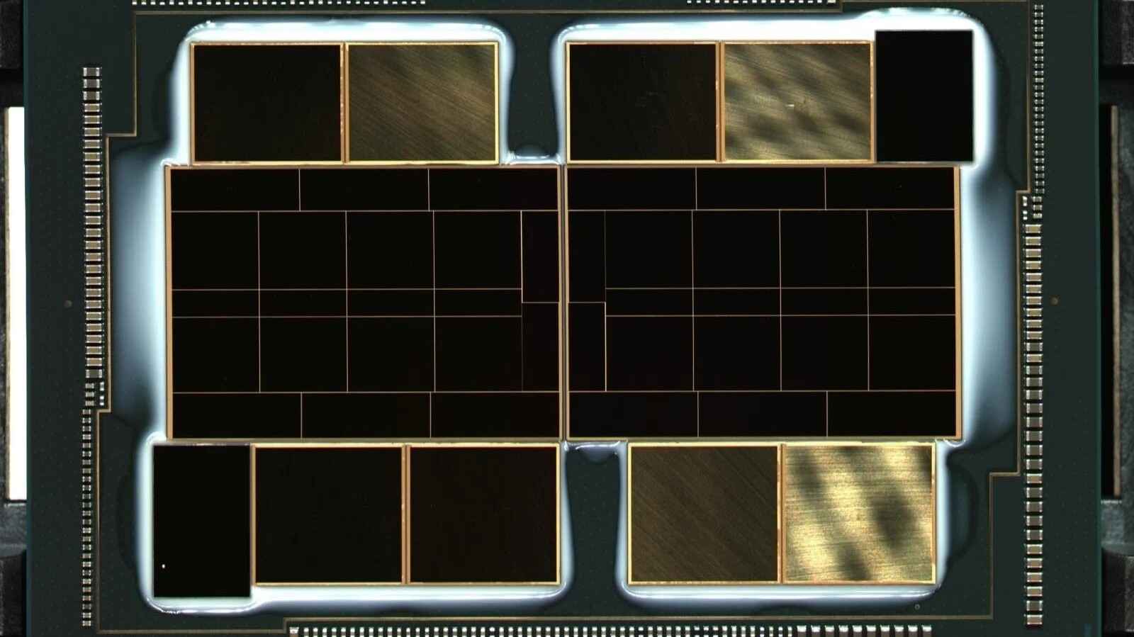
The BGA 2114 design points to a mobile processor platform, and industry analysts are fairly certain that Intel is preparing next generation high-end laptop CPUs in the form of its rumored Arrow Lake-HX lineup. This range is set to succeed the 13th generation Core-HX Raptor Lake family of mobile processors. The new BGA package looks to be slightly larger than the closest predecessor, possibly accommodating Intel's new "disaggregated" tile-based (tile is their term for chiplet) internal layout.

Intel Meteor Lake to Feature 50% Increase in Efficiency, 2X Faster iGPU

Intel's upcoming Meteor Lake processor family is supposedly looking good with the new performance/efficiency targets. According to the @OneRaichu Twitter account, we have a potential performance estimate for the upcoming SKUs. As the latest information notes, Intel's 14th-generation Meteor Lake will feature around a 50% increase in efficiency compared to the 13th-generation Raptor Lake designs. This means that the processor can use half the power at the same performance target at Raptor Lake, increasing efficiency. Of course, the design also offers some performance improvements besides efficiency that are significant and are yet to be shown. The new Redwood Cove P-cores will be combined with the new Crestmont E-cores for maximum performance inside U/P/H configurations with 15-45 Watt power envelopes.

For integrated graphics, the source notes that Meteor Lake offers twice the performance of iGPU found on Raptor Lake designs. Supposedly, Meteor Lake will feature 128 EUs running 2.0+GHz compared to 96 EUs found inside Raptor Lake. The iGPU architecture will switch from Intel Iris to Xe-LPG 'Xe-MTL' family on the 14th gen models, confirming a giant leap in performance that iGPU is supposed to experience. Using the tile-based design, Intel combines the Intel 4 process for the CPU tile and the TSMC 5 nm process for the GPU tile. Intel handles final packaging for additional tuning, and you can see the separation below.

Alleged AMD Instinct MI300 Exascale APU Features Zen4 CPU and CDNA3 GPU

Today we got information that AMD's upcoming Instinct MI300 will be allegedly available as an Accelerated Processing Unit (APU). AMD APUs are processors that combine CPU and GPU into a single package. AdoredTV managed to get ahold of a slide that indicates that AMD Instinct MI300 accelerator will also come as an APU option that combines Zen4 CPU cores and CDNA3 GPU accelerator in a single, large package. With technologies like 3D stacking, MCM design, and HBM memory, these Instinct APUs are positioned to be a high-density compute the product. At least six HBM dies are going to be placed in a package, with the APU itself being a socketed design.

The leaked slide from AdoredTV indicates that the first tapeout is complete by the end of the month (presumably this month), with the first silicon hitting AMD's labs in Q3 of 2022. If the silicon turns out functional, we could see these APUs available sometime in the first half of 2023. Below, you can see an illustration of the AMD Instinct MI300 GPU. The APU version will potentially be of the same size with Zen4 and CDNA3 cores spread around the package. As Instinct MI300 accelerator is supposed to use eight compute tiles, we could see different combinations of CPU/GPU tiles offered. As we await the launch of the next-generation accelerators, we are yet to see what SKUs AMD will bring.

Intel Meteor Lake, HBM2E-enabled Sapphire Rapids, and Ponte Vecchio Pictured

Intel has allowed the media to get a closer look at the next generation of silicon that will power millions of systems in years to come during its private Vision event. PC Watch, a Japanese tech media, managed to get some shots of the upcoming Meteor Lake, Sapphire Rapids, and Ponte Vecchio processors. Starting with Meteor Lake, Intel has displayed two packages for this processor family. The first one is the ultra-compact, high-density UP9 package used for highly compact mobile systems, and it is made out of silicon with minimal packaging to save space. The second one is a traditional design with more oversized packaging, designed for typical laptop/notebook configurations.

Intel Details Ponte Vecchio Accelerator: 63 Tiles, 600 Watt TDP, and Lots of Bandwidth

During the International Solid-State Circuits Conference (ISSCC) 2022, Intel gave us a more significant look at its upcoming Ponte Vecchio HPC accelerator and how it operates. So far, Intel convinced us that the company created Ponte Vecchio out of 47 tiles glued together in one package. However, the ISSCC presentation shows that the accelerator is structured rather interestingly. There are 63 tiles in total, where 16 are reserved for compute, eight are used for RAMBO cache, two are Foveros base tiles, two represent Xe-Link tiles, eight are HBM2E tiles, and EMIB connection takes up 11 tiles. This totals for about 47 tiles. However, an additional 16 thermal tiles used in Ponte Vecchio regulate the massive TDP output of this accelerator.

What is interesting is that Intel gave away details of the RAMBO cache. This novel SRAM technology uses four banks of 3.75 MB groups total of 15 MB per tile. They are connected to the fabric at 1.3 TB/s connection per chip. In contrast, compute tiles are connected at 2.6 TB/s speeds to the chip fabric. With eight RAMBO cache tiles, we get an additional 120 MB SRAM present. The base tile is a 646 mm² die manufactured in Intel 7 semiconductor process and contains 17 layers. It includes a memory controller, the Fully Integrated Voltage Regulators (FIVR), power management, 16-lane PCIe 5.0 connection, and CXL interface. The entire area of Ponte Vecchio is rather impressive, as 47 active tiles take up 2,330 mm², whereas when we include thermal dies, the total area jumps to 3,100 mm². And, of course, the entire package is much larger at 4,844 mm², connected to the system with 4,468 pins.

Tile Unveils New Products, Introduces New Features to Make Finding Easier for Everyone

Tile, the pioneer in finding technology, introduces a new lineup that builds on the superior features consumers around the world rely on to keep track of their things. Available today, the lineup includes sleek new designs for a wide range of uses, increased finding range, louder ring and a new way for lost items to be found and returned. The company will also be introducing highly accurate Point and Locate finding with the launch of the Ultra-Wideband enabled Tile Ultra as well as a new Scan and Secure safety feature early next year.

Tile is built for everyone and everything, with a platform agnostic app and multiple form factors that attach to just about anything right out of the box. At a time when consumers are faced with even more choice within the category, Tile continues to see significant growth, a testament to its wide appeal. In the first half of 2021, Tile has grown revenue over 50 percent, and shows no sign of slowing down.

Intel Accelerates Packaging and Process Innovations

Intel Corporation today revealed one of the most detailed process and packaging technology roadmaps the company has ever provided, showcasing a series of foundational innovations that will power products through 2025 and beyond. In addition to announcing RibbonFET, its first new transistor architecture in more than a decade, and PowerVia, an industry-first new backside power delivery method, the company highlighted its planned swift adoption of next-generation extreme ultraviolet lithography (EUV), referred to as High Numerical Aperture (High NA) EUV. Intel is positioned to receive the first High NA EUV production tool in the industry.

"Building on Intel's unquestioned leadership in advanced packaging, we are accelerating our innovation roadmap to ensure we are on a clear path to process performance leadership by 2025," Intel CEO Pat Gelsinger said during the global "Intel Accelerated" webcast. "We are leveraging our unparalleled pipeline of innovation to deliver technology advances from the transistor up to the system level. Until the periodic table is exhausted, we will be relentless in our pursuit of Moore's Law and our path to innovate with the magic of silicon."

Intel Ponte Vecchio GPU to Be Liquid Cooled Inside OAM Form Factor

Intel's upcoming Ponte Vecchio graphics card is set to be the company's most powerful processor ever designed, and the chip is indeed looking like an engineering marvel. From Intel's previous teasers, we have learned that Ponte Vecchio is built using 47 "magical tiles" or 47 dies which are responsible either for computing elements, Rambo Cache, Xe links, or something else. Today, we are getting a new piece of information coming from Igor's LAB, regarding the Ponte Vecchio and some of its design choices. For starters, the GPU will be a heterogeneous design that consists out of many different nodes. Some parts of the GPU will be manufactured on Intel's 10 nm SuperFin and 7 nm technologies, while others will use TSMC's 7 nm and 5 nm nodes. The smaller and more efficient nodes will probably be used for computing elements. Everything will be held together by Intel's EMIB and Foveros 3D packaging.

Next up, we have information that this massive Intel processor will be accountable for around 600 Watts of heat output, which is a lot to cool. That is why in the leaked renders, we see that Intel envisioned these processors to be liquid-cooled, which would make the cooling much easier and much more efficient compared to air cooling of such a high heat output. Another interesting thing is that the Ponte Vecchio is designed to fit inside OAM (OCP Accelerator Module) form factor, an alternative to the regular PCIe-based accelerators in data centers. OAM is used primarily by hyper scalers like Facebook, Amazon, Google, etc., so we imagine that Intel already knows its customers before the product even hits the market.

EK Water Blocks Updates EK-Classic Water Cooling Kits

EK, the premium liquid cooling gear manufacturer, is updating EK-Classic Kits by rolling out a special Black Nickel Edition, and that's not where the magic ends. These new, special edition, Classic kits are available for the same price as the previous Classic kits, even though there are now more fittings included.

EK-Classic CPU Water Block 115x/20xx/AM4 D-RGB - a high-end, nickel-plated copper CPU water block for modern Intel and AMD processors. It uses addressable RGB LEDs to light up your CPU area. It features a classic, market-proven design that will perfectly fit the needs of enthusiasts and demanding users. The tool-less mounting system makes the installation process a breeze even for beginners. This block comes with a pre-installed Intel mounting system while the AMD AM4 mounting system is in the packaging and needs to be installed if needed.

Raja Koduri Previews "PetaFLOPs Scale" 4-Tile Intel Xe HP GPU

Raja Koduri, Intel's chief architect and senior vice president of Intel's discrete graphics division, has today held a talk at HotChips 32, the latest online conference of 2020, that shows off the latest architectural advancements in the semiconductor industry. So Intel has prepared two talks, one about Ice Lake-SP server CPUs and one about Intel's efforts in the upcoming graphics card launch. So what has Intel been working on the whole time? Raja Koduri took over the talk and has benchmarked the upcoming GPU and recorded how much raw power the GPUs posses, possibly counting in PetaFLOPs.

When Mr. Koduri got to talk, he pulled the 4-tile Xe HP GPU out of his pocket and showed for the first time how the chip looks. And it is one big chip. Featuring 4 tiles, the GPU represents Intel's fastest and biggest variant of Xe HP GPUs. The benchmark Intel ran was made to show off scaling on the Xe architecture and how the increase in the number of tiles results in a scalable increase in performance. Running on a single tile, the GPU managed to develop the performance of 10588 GFLOPs or around 10.588 TeraFLOPs. When there are two tiles, the performance scales almost perfectly at 21161 GFLOPS (21.161 TeraFLOPs) for 1.999X improvement. At four tiles the GPU achieves 3.993 times scaling and scores 41908 GFLOPs resulting in 41.908 TeraFLOPS, all measured in single-precision FP32.
Intel Xe HP GPU Demo Intel Xe HP GPU Demo Intel Xe HP GPU Demo

CEA-Leti Makes a 96 core CPU from Six Chiplets

Chiplet design of processors is getting more popular due to many improvements and opportunities it offers. Some of the benefits include lower costs as the dies are smaller compared to one monolithic design, while you are theoretically able to stitch as much of the chiplets together as possible. During the ISSCC 2020 conference, CEA-Leti, a French research institute, created a 96 core CPU made from six 3D stacked 16 core chiplets. The chip is created as a demonstration of what this modular approach offers and what are the capabilities of the chiplet-based CPU design.

The chiplets are manufactured on the 28 nm FD-SOI manufacturing process from STMicroelectronics, while the active interposer die below them that is connecting everything is made using the 65 nm process. Each one of the six dies is housing 16 cores based on MIPS Instruction Set Architecture core. Each chiplet is split into four 4-core clusters that make up for a total of 16 cores per chiplet. When it comes to the core itself, it is a scalar MIPS32v1 core equipped with 16 KiB of L1 instruction and an L1 data cache. For L2 cache, there is 256 KiB per cluster, while the L3 cache is split into four 1 MiB tiles for the whole cluster. The chiplets are stacked on top of an active interposer which connects the chiplets and provides external I/O support.

Intel Xe Graphics to Feature MCM-like Configurations, up to 512 EU on 500 W TDP

A reportedly leaked Intel slide via DigitalTrends has given us a load of information on Intel's upcoming take on the high performance graphics accelerators market - whether in its server or consumer iterations. Intel's Xe has already been cause for much discussion in a market that has only really seen two real competitors for ages now - the coming of a third player with muscles and brawl such as Intel against the already-established players NVIDIA and AMD would surely spark competition in the segment - and competition is the lifeblood of advancement, as we've recently seen with AMD's Ryzen CPU line.

The leaked slide reveals that Intel will be looking to employ a Multi-Chip-Module (MCM) approach to its high performance "Arctic Sound" graphics architecture. The GPUs will be available in up to 4-tile configuration (the name Intel is giving each module), which will then be joined via Foveros 3D stacking (first employed in Intel Lakefield. This leaked slide shows Intel's approach starting with a 1-tile GPU (with only 96 of its 128 total EUs active) for the entry level market (at 75 W TDP) a-la DG1 SDV (Software Development Vehicle).
Return to Keyword Browsing
Apr 25th, 2024 02:14 EDT change timezone

New Forum Posts

Popular Reviews

Controversial News Posts