Thursday, February 12th 2009

Samsung Begins Production of High-performance GDDR5 Memory Using 50-nm Technology
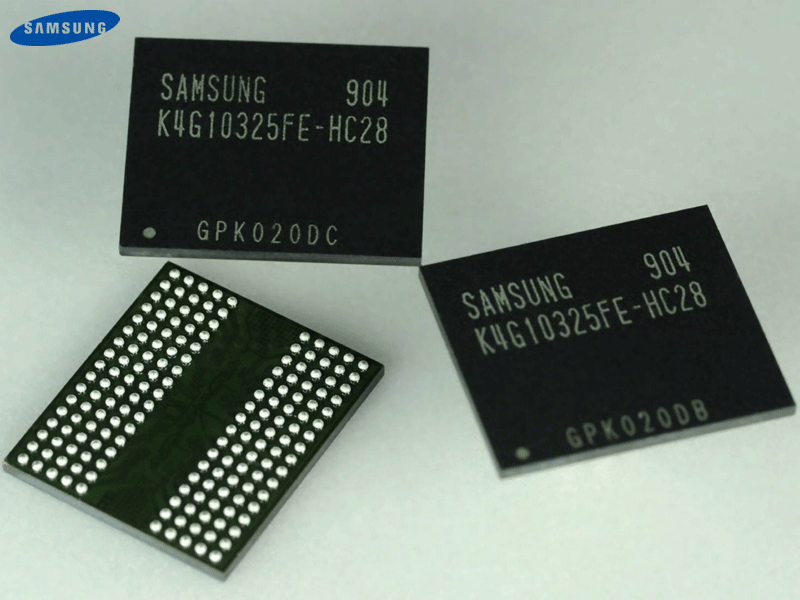
Samsung Electronics Co., Ltd., the world leader in advanced memory technology and the leading producer of high-end graphics memory, announced today that it has begun mass producing GDDR5 graphics memory using 50-nanometer class process technology.
"Our early 2009 introduction of GDDR5 chips will help us to meet the growing demand for higher performance graphics memory in PCs, graphic cards and game consoles," said Mueez Deen, director, mobile and graphics memory, Samsung Semiconductor, Inc. "Because GDDR5 is the fastest and highest performing memory in the world, we're able to improve the gaming experience with it across all platforms," he added. Designed to support a maximum data transfer speed of 7.0Gbps, Samsung's GDDR5 will render more life-like (3D) imaging with a maximum 28GB/s bandwidth, which is more than twice that of the previous fastest graphics memory bandwidth of 12.8GB/s for GDDR4. The ultra-fast processing speed is equivalent to transferring nineteen 1.5GB DVD resolution movies in one second. The high image processing speed of the GDDR5 also supports the latest data formats (Blu-ray and full HD).
Unlike GDDR4, which processes data and images using the strobe-and-clock technique, the processing speed of the GDDR5 is much faster because it operates with a free-running clock that does not require the data read/write function to be synchronized to the operations of the clock. By adopting 50nm class technology, Samsung expects production efficiency to rise 100 percent over 60nm class technology. In addition, Samsung's GDDR5 operates at 1.35 volts (V), which represents a 20 percent reduction in power consumption compared to the 1.8V at which GDDR4 devices operate.
Now available in a 32Megabit (Mb) x32 configuration and also configurable as a 64Mb x16 device, Samsung expects GDDR5 to account for over 20 percent of the total graphic memory market in 2009. The company also said it plans to expand the 50-nm process technology throughout its graphics memory line-up this year.
Source:
Samsung
"Our early 2009 introduction of GDDR5 chips will help us to meet the growing demand for higher performance graphics memory in PCs, graphic cards and game consoles," said Mueez Deen, director, mobile and graphics memory, Samsung Semiconductor, Inc. "Because GDDR5 is the fastest and highest performing memory in the world, we're able to improve the gaming experience with it across all platforms," he added.
Unlike GDDR4, which processes data and images using the strobe-and-clock technique, the processing speed of the GDDR5 is much faster because it operates with a free-running clock that does not require the data read/write function to be synchronized to the operations of the clock. By adopting 50nm class technology, Samsung expects production efficiency to rise 100 percent over 60nm class technology. In addition, Samsung's GDDR5 operates at 1.35 volts (V), which represents a 20 percent reduction in power consumption compared to the 1.8V at which GDDR4 devices operate.
Now available in a 32Megabit (Mb) x32 configuration and also configurable as a 64Mb x16 device, Samsung expects GDDR5 to account for over 20 percent of the total graphic memory market in 2009. The company also said it plans to expand the 50-nm process technology throughout its graphics memory line-up this year.
26 Comments on Samsung Begins Production of High-performance GDDR5 Memory Using 50-nm Technology
Looks good to me though.
Increasing the bus does not cost money.
Would be nice to see how this ram would do on a 4870 x2 lol.
If either one leads too far ahead of the other its just a total waste overall.
The only real solution would be to integrate the ram & the gpu .. see what ppl seem to forget is that electronic impulses take TIME to travel along the tracks on a PCB.. .the real enemy here is the distance between the ram and the GPU.
Once you start working at the multi-gigahertz level, even the extra time taken for that pulse to travel an extra half an inch can be a significant problem.
Until we start putting the two closer together, there really are real-world physics based limitations that the designers have to deal with, and cant avoid.
(See : Intel moving nothbridge into CPU & others)
Technology is getting to the point where manufacturer's are limited by the electrical connections to devices. The only cheap and easy solution to that is parallel lanes. They have come up with some ideas like BGA connection to the PCB and LGA sockets. Back in the 478 days Intel told me the 478 socket had a limit of 4ghz before the pins became "little antennas" as they said.
Videocards have 256bit memory address. Why so wide? Why not just make faster ram? Because you can't get the performance out of it that's why.
To get back on topic, it is a good thing to see lower power consumption. This leads to higher speeds. You have to remember that they can't jump too far ahead or they'll loose money. If ATI made say a 4870x12 single slot card, and charged $200 for it, what would that do to the graphics market? It would be ruined. We'd all own 2 of them and not need an upgrade for 5 years.
They won't make something like 512bit memory addressing anyways because they feel we dont need it yet. It's all marketing. We get the more profitable technology available. Not the fastest.
And $1 across millions of boards adds up pretty quickly. It's still significant, and that likely only covers the material costs, and not the tooling costs. Overall, the 512bit bus with GDDR3 is more expensive to both develop and manufacture than the 256bit bus with GDDR5.