Report an Error


NVIDIA TU104
TU104
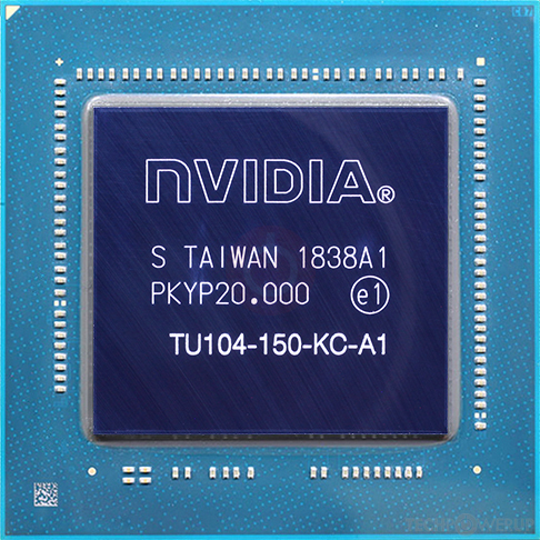
TU104-150-KC-A1

TU104-400A-A1

TU104-410-A1

TU104-450-A1
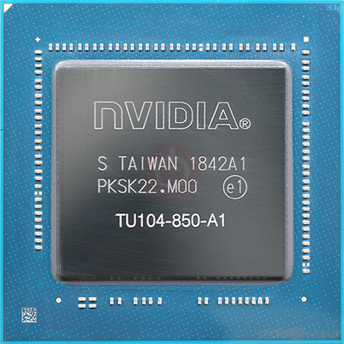
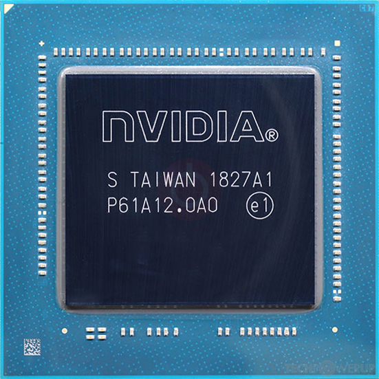
TU104-850-A1

N18E-G3-A1

Fritzchens Fritz
Die Shot

Block Diagram

SM Diagram
NVIDIA's TU104 GPU uses the Turing architecture and is made using a 12 nm production process at TSMC. With a die size of 545 mm² and a transistor count of 13,600 million it is a very big chip. TU104 supports DirectX 12 Ultimate (Feature Level 12_2). For GPU compute applications, OpenCL version 3.0 and CUDA 7.5 can be used. Additionally, the DirectX 12 Ultimate capability guarantees support for hardware-raytracing, variable-rate shading and more, in upcoming video games. It features 3072 shading units, 192 texture mapping units and 64 ROPs. Also included are 384 tensor cores which help improve the speed of machine learning applications. The GPU also contains 48 raytracing acceleration cores.
Further reading:
Turing Architecture Whitepaper 
Graphics Processor
- Released
- Aug 13th, 2018
- GPU Name
- TU104
- Codename
- NV164
- Architecture
- Turing
- Foundry
- TSMC
- Process Type
- 12FFN FinFET
- Process Size
- 12 nm
- Transistors
- 13,600 million
- Density
- 25.0M / mm²
- Die Size
- 545 mm²
- Package
- BGA-2228
- Package Size
- 37.5 mm × 37.5 mm
Graphics Features
- DirectX
- 12 Ultimate (12_2)
- OpenGL
- 4.6
- OpenCL
- 3.0
- Vulkan
- 1.3
- CUDA
- 7.5
- Shader Model
- 6.8
- WDDM
- 3.2
- Tensor Cores
- 2nd Gen
- RT Cores
- 1st Gen
- NVENC
- 7th Gen
- NVDEC
- 4th Gen
- PureVideo HD
- VP10
- VDPAU
- Feature Set J
Render Config
- Shading Units
- 3072
- TMUs
- 192
- ROPs
- 64
- SM Count
- 48
- FP16 Units
- 6144
- FP64 Units
- 96
- INT32 Units
- 3072
- Tensor Cores
- 384
- RT Cores
- 48
- SFUs
- 768
- TPCs
- 24
- GPCs
- 6
- Tex L1 Cache
- 32 KB per SM
- L1 Cache
- 64 KB per SM
- L2 Cache
- 4096 KB
- Max. TDP
- 250 W
All Turing GPUs
NVIDIA GPU Architecture History
- 2025 Blackwell 2.0
- 2024 Blackwell
- 2022-2024 Hopper
- 2022-2024 Ada Lovelace
- 2020-2024 Ampere
- 2018-2022 Turing
- 2017-2020 Volta
- 2016-2021 Pascal
- 2014-2019 Maxwell 2.0
- 2014-2017 Maxwell
- 2013-2015 Kepler 2.0
- 2012-2018 Kepler
- 2010-2016 Fermi 2.0
- 2010-2013 VLIW Vec4
- 2010-2016 Fermi
- 2007-2013 Tesla 2.0
- 2006-2010 Tesla
- 2003-2013 Curie
- 2003-2005 Rankine
- 2001-2003 Kelvin
- 1999-2005 Celsius
- 1998-2000 Fahrenheit
Graphics cards using the NVIDIA TU104 GPU
| Name | Chip | Memory | Shaders | TMUs | ROPs | Base Clock | Boost Clock | Memory Clock |
|---|---|---|---|---|---|---|---|---|
| TU104-400A-A1 | 8 GB | 2944 | 184 | 64 | 1515 MHz | 1710 MHz | 1750 MHz | |
| TU104-875-A1 | 16 GB | 3072 | 192 | 64 | 1620 MHz | 1815 MHz | 1750 MHz | |
| N18E-G3-A1 | 8 GB | 2944 | 184 | 64 | 1380 MHz | 1590 MHz | 1750 MHz | |
| TU104-895-A1 | 16 GB | 2560 | 160 | 64 | 585 MHz | 1590 MHz | 1250 MHz | |
| TU104-850-A1 | 8 GB | 2304 | 144 | 64 | 1005 MHz | 1545 MHz | 1625 MHz | |
| N18E-G3-A1 | 8 GB | 2944 | 184 | 64 | 735 MHz | 1095 MHz | 1500 MHz | |
| 8 GB | 2560 | 160 | 64 | 780 MHz | 1380 MHz | 1500 MHz | ||
| N19E-Q3-A1 | 8 GB | 2560 | 160 | 64 | 1110 MHz | 1560 MHz | 1750 MHz | |
| N19E-Q5-A1 | 16 GB | 3072 | 192 | 64 | 1035 MHz | 1530 MHz | 1750 MHz | |
| 16 GB | 3072 | 192 | 64 | 600 MHz | 1350 MHz | 1500 MHz | ||
| TU104-450-A1 | 8 GB | 3072 | 192 | 64 | 1650 MHz | 1815 MHz | 1937 MHz | |
| TU104-410-A1 | 8 GB | 2560 | 160 | 64 | 1605 MHz | 1770 MHz | 1750 MHz | |
| TU104-150-KC-A1 | 6 GB | 1920 | 120 | 48 | 1365 MHz | 1680 MHz | 1750 MHz | |
| N18E-G3-A1 | 8 GB | 3072 | 192 | 64 | 1365 MHz | 1560 MHz | 1750 MHz | |
| N18E-G2R | 8 GB | 2560 | 160 | 64 | 1140 MHz | 1380 MHz | 1750 MHz | |
| 8 GB | 2560 | 160 | 64 | 930 MHz | 1155 MHz | 1375 MHz | ||
| N18E-G3R | 8 GB | 3072 | 192 | 64 | 735 MHz | 975 MHz | 1375 MHz | |
| TU104-400A-A1 | 8 GB | 3072 | 192 | 64 | 1515 MHz | 1710 MHz | 1750 MHz | |
| N19E-Q5-A1 | 16 GB | 3072 | 192 | 64 | 1035 MHz | 1530 MHz | 1750 MHz | |
| 16 GB | 2560 | 160 | 64 | 585 MHz | 1590 MHz | 1250 MHz |


TU104 GPU Notes
| Ray Tracing Cores: 1st Gen Tensor Cores: 2nd Gen NVENC: 7th Gen NVDEC: 4th Gen PureVideo HD: VP10 VDPAU: Feature Set J Latest Drivers: Windows 7 / 8 / 8.1 (x64): GeForce Release 474.89 Quadro Release R440 U3 (441.28) Data Center Release 426.32 Windows 10 / 11 (x64): GeForce Release: Latest Quadro Release: Latest Data Center Release: Latest |
Jun 27th, 2025 10:36 CDT
change timezone
Latest GPU Drivers
New Forum Posts
- Current Sales, Bundles, Giveaways (10339)
- PC and monitor randomly restarts , like power goes and comes very fast ( both plugged on a line filter ) (17)
- MSI Titan 18 Dragon Edition (Norse Myth) Intel 285HX Optimisation (4)
- Have you got pie today? (16763)
- What's your latest tech purchase? (24142)
- Best time to sell your used 4090s is now. (237)
- Router with removable antennas & custom F/W capability (13)
- vBios for RTX 5080 PALIT GamingPro (0)
- PCIe5(AM5) vs PCIe4(AM4) (16)
- Technical considerations about how to convert a sensor from I2C to USB. (16)
Popular Reviews
- ASRock Phantom Gaming Z890 Riptide Wi-Fi Review
- Sapphire Radeon RX 9060 XT Pulse OC 16 GB Review - Samsung Memory Tested
- SCHENKER KEY 18 Pro (E25) Review - Top-Tier Contender
- AMD Ryzen 7 9800X3D Review - The Best Gaming Processor
- Upcoming Hardware Launches 2025 (Updated May 2025)
- Lexar NQ780 4 TB Review
- Sapphire Radeon RX 9070 XT Nitro+ Review - Beating NVIDIA
- NVIDIA GeForce RTX 5060 8 GB Review
- Intel Core Ultra 7 265K Review
- AMD Ryzen 9 9950X3D Review - Great for Gaming and Productivity
TPU on YouTube
Controversial News Posts
- Intel's Core Ultra 7 265K and 265KF CPUs Dip Below $250 (283)
- NVIDIA Grabs Market Share, AMD Loses Ground, and Intel Disappears in Latest dGPU Update (203)
- Microsoft Partners with AMD for Next-gen Xbox Hardware (105)
- NVIDIA Launches GeForce RTX 5050 for Desktops and Laptops, Starts at $249 (101)
- Intel "Nova Lake‑S" Series: Seven SKUs, Up to 52 Cores and 150 W TDP (100)
- Reviewers Bemused by Restrictive Sampling of RX 9060 XT 8 GB Cards (88)
- NVIDIA GeForce RTX 5050 Reportedly Scheduled for July Release (87)
- GPU IPC Showdown: NVIDIA Blackwell vs Ada Lovelace; AMD RDNA 4 vs RDNA 3 (78)