Report an Error


NVIDIA G92B

G92B

G92-159-B1
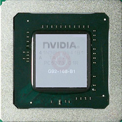
G92-168-B1

G92-280-B1

G92-420-B1

G92-421-B1

G92-426-B1
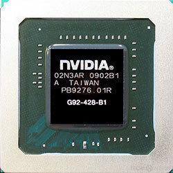
G92-428-B1

N10E-GLM3-B2

N10E-GTX1-B1

G92 BGA
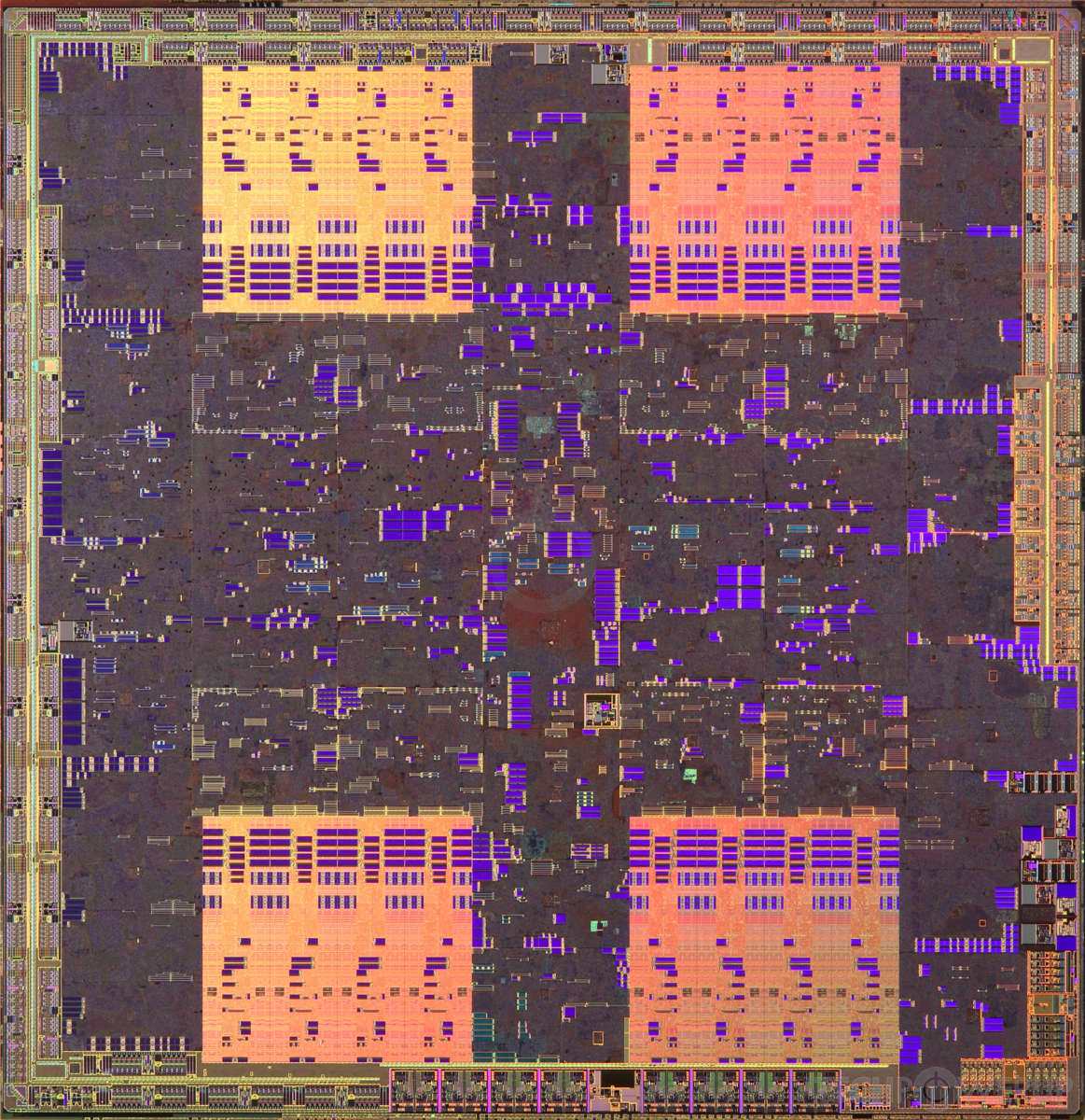
Die Shot

TPC Diagram
NVIDIA's G92B GPU uses the Tesla architecture and is made using a 55 nm production process at TSMC. With a die size of 260 mm² and a transistor count of 754 million it is a medium-sized chip. G92B supports DirectX 11.1 (Feature Level 10_0). For GPU compute applications, OpenCL version 1.1 and CUDA 1.1 can be used. It features 128 shading units, 64 texture mapping units and 16 ROPs.
Further reading:
Tesla Architecture Whitepaper 
Graphics Processor
- Released
- Jul 21st, 2008
- GPU Name
- G92B
- Codename
- NV92
- Architecture
- Tesla
- Foundry
- TSMC
- Process Size
- 55 nm
- Transistors
- 754 million
- Density
- 2.9M / mm²
- Die Size
- 260 mm²
- Package
- FCBGA-1148
Graphics Features
- DirectX
- 11.1 (10_0)
- OpenGL
- 3.3
- OpenCL
- 1.1
- Vulkan
- N/A
- CUDA
- 1.1
- Shader Model
- 4.0
- WDDM
- 1.2
- PureVideo HD
- VP2
- VDPAU
- Feature Set A
Render Config
- Shading Units
- 128
- TMUs
- 64
- ROPs
- 16
- SM Count
- 16
- SFUs
- 32
- TPCs
- 8
- Tex L1 Cache
- 16 KB per TPC
- L2 Cache
- 64 KB
- Max. TDP
- 150 W
All Tesla GPUs
NVIDIA GPU Architecture History
- 2024 Blackwell
- 2023 Hopper
- 2022-2024 Ada Lovelace
- 2020-2024 Ampere
- 2018-2022 Turing
- 2017-2020 Volta
- 2016-2021 Pascal
- 2014-2019 Maxwell 2.0
- 2014-2017 Maxwell
- 2013-2015 Kepler 2.0
- 2012-2018 Kepler
- 2010-2016 Fermi 2.0
- 2010-2013 VLIW Vec4
- 2010-2016 Fermi
- 2007-2013 Tesla 2.0
- 2006-2010 Tesla
- 2003-2013 Curie
- 2003-2005 Rankine
- 2001-2003 Kelvin
- 1999-2005 Celsius
- 1998-2000 Fahrenheit
Graphics cards using the NVIDIA G92B GPU
| Name | Chip | Memory | Shaders | TMUs | ROPs | GPU Clock | Memory Clock |
|---|---|---|---|---|---|---|---|
| G92-420-B1 | 512 MB | 128 | 64 | 16 | 738 MHz | 1100 MHz | |
| G92-428-B1 | 1024 MB | 128 | 64 | 16 | 702 MHz | 1000 MHz | |
| G92-240-B1 | 1024 MB | 112 | 56 | 16 | 675 MHz | 1100 MHz | |
| N10E-GTX1-B1 | 1024 MB | 128 | 64 | 16 | 600 MHz | 1000 MHz | |
| G92-159-B1 | 1536 MB | 96 | 48 | 12 | 500 MHz | 500 MHz | |
| N10E-GLM3-B2 | 1024 MB | 128 | 64 | 16 | 675 MHz | 1000 MHz | |
| N10E-GLM-B2 | 1024 MB | 96 | 48 | 16 | 600 MHz | 1000 MHz | |
| G92-168-B1 | 256 MB | 96 | 48 | 16 | 500 MHz | 510 MHz | |
| G92-280-B1 | 512 MB | 112 | 56 | 16 | 600 MHz | 900 MHz | |
| G92-426-B1 | 1024 MB | 128 | 64 | 16 | 675 MHz | 1008 MHz |


G92B GPU Notes
| PureVideo HD: VP2 VDPAU: Feature Set A |
Apr 26th, 2024 23:06 EDT
change timezone
Latest GPU Drivers
New Forum Posts
- Black screens leading to restarts (Event ID 18) on AMD platform since changing graphics card (43)
- FINAL FANTASY XIV: Dawntrail Official Benchmark (73)
- Your PC ATM (34509)
- Rare GPUs / Unreleased GPUs (1877)
- looking to build a new system and im considering asrock brand but i have some doubts/concerns. (15)
- AAF Optimus DCH Audio Modded Driver for Windows 10/11 - For ALL HDAUDIO Enumerator Chips (652)
- Help me identify rx 580 card ? (0)
- Strange system crashes out of nowhere help (9)
- What phone you use as your daily driver? And, a discussion of them. (1494)
- Secure boot already open help (11)
Popular Reviews
- Ugreen NASync DXP4800 Plus Review
- HYTE THICC Q60 240 mm AIO Review
- Quick Look: MOONDROP CHU 2 Budget In-Ear Monitors
- MOONDROP x Crinacle DUSK In-Ear Monitors Review - The Last 5%
- Thermalright Phantom Spirit 120 EVO Review
- Upcoming Hardware Launches 2023 (Updated Feb 2024)
- Intel Core i9-14900KS Review - The Last of its Kind
- FiiO K19 Desktop DAC/Headphone Amplifier Review
- Alienware Pro Wireless Gaming Keyboard Review
- CeBIT 2008: Akasa Review
Controversial News Posts
- Windows 11 Now Officially Adware as Microsoft Embeds Ads in the Start Menu (135)
- Sony PlayStation 5 Pro Specifications Confirmed, Console Arrives Before Holidays (117)
- NVIDIA Points Intel Raptor Lake CPU Users to Get Help from Intel Amid System Instability Issues (106)
- AMD "Strix Halo" Zen 5 Mobile Processor Pictured: Chiplet-based, Uses 256-bit LPDDR5X (103)
- US Government Wants Nuclear Plants to Offload AI Data Center Expansion (98)
- AMD's RDNA 4 GPUs Could Stick with 18 Gbps GDDR6 Memory (95)
- Developers of Outpost Infinity Siege Recommend Underclocking i9-13900K and i9-14900K for Stability on Machines with RTX 4090 (85)
- Windows 10 Security Updates to Cost $61 After 2025, $427 by 2028 (84)