Report an Error


NVIDIA EXK107

EXK107
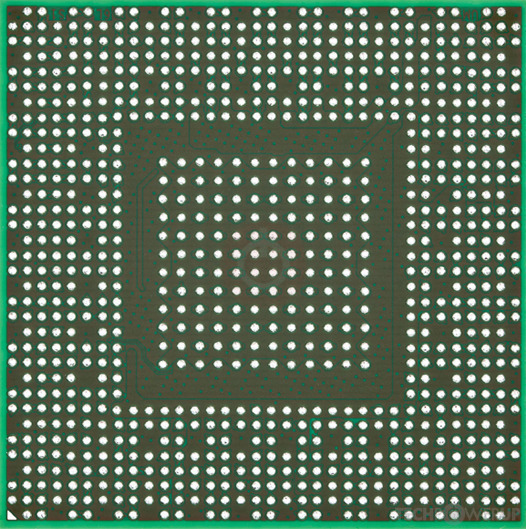
GK107 BGA
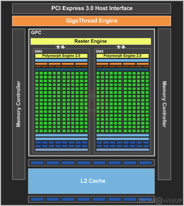
Block Diagram

SM Diagram
NVIDIA's EXK107 GPU uses the Kepler architecture and is made using a 28 nm production process at TSMC. With a die size of 118 mm² and a transistor count of 1,270 million it is a small chip. EXK107 supports DirectX 11.0 (Feature Level 11_0). For GPU compute applications, OpenCL version 3.0 and CUDA 3.0 can be used. It features 384 shading units, 32 texture mapping units and 16 ROPs.
Graphics Processor
- Released
- Mar 22nd, 2012
- GPU Name
- EXK107
- Architecture
- Kepler
- Foundry
- TSMC
- Process Size
- 28 nm
- Transistors
- 1,270 million
- Density
- 10.8M / mm²
- Die Size
- 118 mm²
- Package
- BGA-908
Graphics Features
- DirectX
- 11.0 (11_0)
- OpenGL
- 4.1
- OpenCL
- 3.0
- Vulkan
- N/A
- CUDA
- 3.0
- Shader Model
- 5.1
Render Config
- Shading Units
- 384
- TMUs
- 32
- ROPs
- 16
- SM Count
- 2
- SFUs
- 64
- GPCs
- 1
- Tex L1 Cache
- 48 KB per SMX
- L1 Cache
- 16 KB per SM
- L2 Cache
- 256 KB
- Max. TDP
- 45 W
All Kepler GPUs
NVIDIA GPU Architecture History
- 2024 Blackwell
- 2023 Hopper
- 2022-2024 Ada Lovelace
- 2020-2024 Ampere
- 2018-2022 Turing
- 2017-2020 Volta
- 2016-2021 Pascal
- 2014-2019 Maxwell 2.0
- 2014-2017 Maxwell
- 2013-2015 Kepler 2.0
- 2012-2018 Kepler
- 2010-2016 Fermi 2.0
- 2010-2013 VLIW Vec4
- 2010-2016 Fermi
- 2007-2013 Tesla 2.0
- 2006-2010 Tesla
- 2003-2013 Curie
- 2003-2005 Rankine
- 2001-2003 Kelvin
- 1999-2005 Celsius
- 1998-2000 Fahrenheit
Graphics cards using the NVIDIA EXK107 GPU
| Name | Chip | Memory | Shaders | TMUs | ROPs | Base Clock | Boost Clock | Memory Clock |
|---|---|---|---|---|---|---|---|---|
| 2 GB | 384 | 32 | 16 | 835 MHz | 1058 MHz | 900 MHz |
EXK107 GPU Notes
| L1 Cache is configurable from 16 KB up to 48 KB per SMX |
May 6th, 2024 21:09 EDT
change timezone
Latest GPU Drivers
New Forum Posts
- Gigabyte Aorus Elite AX V2 rev 1.1 BIOS update "AMD AGESA V2 1.2.0.B" (5)
- nvflashk - Flash any BIOS to NVIDIA GPUs - Safe board ID bypass up to 4xxx series (241)
- Only some humans can see refresh rates faster than others, I am one of those humans. (201)
- Cybersecurity - OSINT Software for Linux (1)
- The Official Thermal Interface Material thread (1167)
- RTX 2070 8GB unable to flash (0)
- Update on the whole PC rebooting issue. There was an extra standoff in the case, but now it's crashing even more (3)
- Battery swap for cyberpower UPS (62)
- What's your latest tech purchase? (20449)
- Silly question about upcoming CPU Upgrade (9)
Popular Reviews
- Finalmouse UltralightX Review
- Cougar Hotrod Royal Gaming Chair Review
- Meze Audio LIRIC 2nd Generation Closed-Back Headphones Review
- Upcoming Hardware Launches 2023 (Updated Feb 2024)
- ASRock NUC BOX-155H (Intel Core Ultra 7 155H) Review
- Corsair iCUE Link RX120 RGB 120 mm Fan Review
- AMD Ryzen 7 7800X3D Review - The Best Gaming CPU
- ASUS Radeon RX 7900 GRE TUF OC Review
- Montech Sky Two GX Review
- HYTE THICC Q60 240 mm AIO Review
Controversial News Posts
- Intel Statement on Stability Issues: "Motherboard Makers to Blame" (248)
- Windows 11 Now Officially Adware as Microsoft Embeds Ads in the Start Menu (167)
- AMD to Redesign Ray Tracing Hardware on RDNA 4 (165)
- Sony PlayStation 5 Pro Specifications Confirmed, Console Arrives Before Holidays (118)
- AMD's RDNA 4 GPUs Could Stick with 18 Gbps GDDR6 Memory (114)
- NVIDIA Points Intel Raptor Lake CPU Users to Get Help from Intel Amid System Instability Issues (106)
- AMD Ryzen 9 7900X3D Now at a Mouth-watering $329 (104)
- AMD "Strix Halo" Zen 5 Mobile Processor Pictured: Chiplet-based, Uses 256-bit LPDDR5X (103)