Report an Error


NVIDIA GK110B

GK110B

GK110-301-B1

GK110-350-B1
GK110-425-B1

GK110-430-B1

GK110-890-B1

Fritzchens Fritz
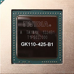
Die Shot

Block Diagram
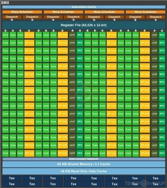
SMX Diagram
NVIDIA's GK110B GPU uses the Kepler architecture and is made using a 28 nm production process at TSMC. With a die size of 561 mm² and a transistor count of 7,080 million it is a very big chip. GK110B supports DirectX 12 (Feature Level 11_1). For GPU compute applications, OpenCL version 3.0 and CUDA 3.5 can be used. It features 2880 shading units, 240 texture mapping units and 48 ROPs.
Further reading:
GK110B Compute Architecture Whitepaper 
Graphics Processor
- Released
- Jul 23rd, 2013
- GPU Name
- GK110B
- Codename
- NVF1
- Architecture
- Kepler
- Foundry
- TSMC
- Process Size
- 28 nm
- Transistors
- 7,080 million
- Density
- 12.6M / mm²
- Die Size
- 561 mm²
- Package
- BGA-2152
Graphics Features
- DirectX
- 12 (11_1)
- OpenGL
- 4.6
- OpenCL
- 3.0
- Vulkan
- 1.2.175
- CUDA
- 3.5
- Shader Model
- 6.5 (5.1)
- WDDM
- 3.0
- NVENC
- 1st Gen
- NVDEC
- 1st Gen
- PureVideo HD
- VP5
- VDPAU
- Feature Set D
Render Config
- Shading Units
- 2880
- TMUs
- 240
- ROPs
- 48
- SMX Count
- 15
- DPUs
- 960
- SFUs
- 480
- GPCs
- 5
- PPC
- 8 per Rasterizer
- Tex L1 Cache
- 48 KB per SMX
- L1 Cache
- 16 KB per SMX
- L2 Cache
- 1536 KB
- Max. TDP
- 375 W
All Kepler GPUs
NVIDIA GPU Architecture History
- 2023 Hopper
- 2022-2024 Ada Lovelace
- 2020-2024 Ampere
- 2018-2022 Turing
- 2017-2020 Volta
- 2016-2021 Pascal
- 2014-2019 Maxwell 2.0
- 2014-2017 Maxwell
- 2013-2015 Kepler 2.0
- 2012-2018 Kepler
- 2010-2016 Fermi 2.0
- 2010-2013 VLIW Vec4
- 2010-2016 Fermi
- 2007-2013 Tesla 2.0
- 2006-2010 Tesla
- 2003-2013 Curie
- 2003-2005 Rankine
- 2001-2003 Kelvin
- 1999-2005 Celsius
- 1998-2000 Fahrenheit
Graphics cards using the NVIDIA GK110B GPU
| Name | Chip | Memory | Shaders | TMUs | ROPs | Base Clock | Boost Clock | Memory Clock |
|---|---|---|---|---|---|---|---|---|
| GK110-890-B1 | 12 GB | 2880 | 240 | 48 | 797 MHz | 902 MHz | 1502 MHz | |
| GK110-425-B1 | 3 GB | 2880 | 240 | 48 | 875 MHz | 928 MHz | 1753 MHz | |
| GK110-300-B1 | 3 GB | 2304 | 192 | 48 | 863 MHz | 902 MHz | 1502 MHz | |
| 12 GB | 2880 | 240 | 48 | 745 MHz | 876 MHz | 1502 MHz | ||
| 12 GB | 2880 | 240 | 48 | 745 MHz | 876 MHz | 1502 MHz | ||
| 12 GB | 2880 | 240 | 48 | 575 MHz | 1502 MHz | |||
| GK110-430-B1 | 6 GB | 2880 | 240 | 48 | 889 MHz | 980 MHz | 1750 MHz | |
| GK110-350-B1 | 6 GB | 2880 | 240 | 48 | 705 MHz | 876 MHz | 1750 MHz | |
| 8 GB | 2304 | 192 | 48 | 667 MHz | 771 MHz | 1502 MHz | ||
| GK110-301-B1 | 6 GB | 2304 | 192 | 48 | 863 MHz | 902 MHz | 1502 MHz | |
| 6 GB | 2880 | 240 | 48 | 875 MHz | 928 MHz | 1753 MHz | ||
| 12 GB | 2880 | 240 | 48 | 745 MHz | 876 MHz | 1502 MHz | ||
| 12 GB | 2880 | 240 | 48 | 745 MHz | 876 MHz | 1502 MHz |


GK110B GPU Notes
| NVENC: 1st Gen NVDEC: 1st Gen PureVideo HD: VP5 VDPAU: Feature Set D L1 Cache is configurable from 16 KB up to 48 KB per SMX GK110B has 5 GPCs each capable of 8 pixels per clock. This limits complete GPU to 40 pixels per clock and because of that it can't feed all 48 ROPs when they all require data at the same time. Additional ROPs however can be used for MSAA (because it doesn't require additional data from rasterizers, while giving more work to ROPs.) |
Apr 26th, 2024 02:52 EDT
change timezone
Latest GPU Drivers
New Forum Posts
- What phone you use as your daily driver? And, a discussion of them. (1484)
- What's your latest tech purchase? (20342)
- Best SSD for system drive (81)
- AMD RX 7000 series GPU Owners' Club (1087)
- im new to throttelstop and i think i messed it up by copying others any hints would be very much aprreciated (3)
- Horizontal black lines popping up on my screen? (4)
- Which new games will you be buying? (316)
- Alphacool CORE 1 CPU block - bulging with danger of splitting? (20)
- Black screen after muting (5)
- What are you playing? (20530)
Popular Reviews
- Fractal Design Terra Review
- Thermalright Phantom Spirit 120 EVO Review
- Corsair 2000D Airflow Review
- ASUS GeForce RTX 4090 STRIX OC Review
- NVIDIA GeForce RTX 4090 Founders Edition Review - Impressive Performance
- ASUS GeForce RTX 4090 Matrix Platinum Review - The RTX 4090 Ti
- MSI GeForce RTX 4090 Suprim X Review
- Gigabyte GeForce RTX 4090 Gaming OC Review
- MSI GeForce RTX 4090 Gaming X Trio Review
- MSI GeForce RTX 4090 Suprim Liquid X Review
Controversial News Posts
- Sony PlayStation 5 Pro Specifications Confirmed, Console Arrives Before Holidays (117)
- Windows 11 Now Officially Adware as Microsoft Embeds Ads in the Start Menu (112)
- NVIDIA Points Intel Raptor Lake CPU Users to Get Help from Intel Amid System Instability Issues (106)
- AMD "Strix Halo" Zen 5 Mobile Processor Pictured: Chiplet-based, Uses 256-bit LPDDR5X (101)
- US Government Wants Nuclear Plants to Offload AI Data Center Expansion (98)
- AMD's RDNA 4 GPUs Could Stick with 18 Gbps GDDR6 Memory (88)
- Developers of Outpost Infinity Siege Recommend Underclocking i9-13900K and i9-14900K for Stability on Machines with RTX 4090 (85)
- Windows 10 Security Updates to Cost $61 After 2025, $427 by 2028 (84)