Report an Error


AMD Radeon HD 6870 X2
- Graphics Processor
- Barts x2
- Cores
- 1120 x2
- TMUs
- 56 x2
- ROPs
- 32 x2
- Memory Size
- 1024 MB x2
- Memory Type
- GDDR5
- Bus Width
- 256 bit x2

GPU
I/O

Top

Bottom

Back
Recommended Gaming Resolutions:
- 1600x900
- 1920x1080
- 2560x1440
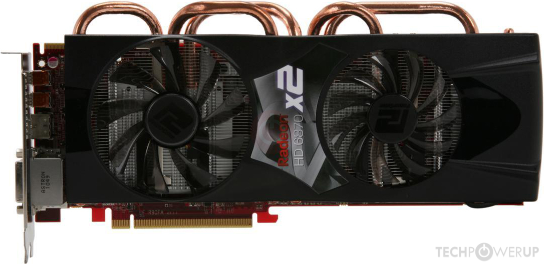
The Radeon HD 6870 X2 was a high-end graphics card by AMD, launched on July 8th, 2011. Built on the 40 nm process, and based on the Barts graphics processor, in its Barts XT variant, the card supports DirectX 11.2. The Barts graphics processor is an average sized chip with a die area of 255 mm² and 1,700 million transistors. Radeon HD 6870 X2 combines two graphics processors to increase performance. It features 1120 shading units, 56 texture mapping units, and 32 ROPs, per GPU. AMD has paired 2,048 MB GDDR5 memory with the Radeon HD 6870 X2, which are connected using a 256-bit memory interface per GPU (each GPU manages 1,024 MB). The GPU is operating at a frequency of 900 MHz, memory is running at 1050 MHz (4.2 Gbps effective).
Being a dual-slot card, the AMD Radeon HD 6870 X2 draws power from 2x 8-pin power connectors, with power draw rated at 300 W maximum. Display outputs include: 2x DVI, 1x HDMI 1.3a, 2x mini-DisplayPort 1.1. Radeon HD 6870 X2 is connected to the rest of the system using a PCI-Express 2.0 x16 interface. The card measures 304 mm in length, and features a dual-slot cooling solution. Its price at launch was 520 US Dollars.
Being a dual-slot card, the AMD Radeon HD 6870 X2 draws power from 2x 8-pin power connectors, with power draw rated at 300 W maximum. Display outputs include: 2x DVI, 1x HDMI 1.3a, 2x mini-DisplayPort 1.1. Radeon HD 6870 X2 is connected to the rest of the system using a PCI-Express 2.0 x16 interface. The card measures 304 mm in length, and features a dual-slot cooling solution. Its price at launch was 520 US Dollars.
Graphics Processor
- GPU Name
- Barts
- GPU Variant
-
Barts XT
(215-0798000)
- Architecture
- TeraScale 2
- Foundry
- TSMC
- Process Size
- 40 nm
- Transistors
- 1,700 million
- Density
- 6.7M / mm²
- Die Size
- 255 mm²
- Chip Package
- HFCBGA-1737
Graphics Card
- Release Date
- Jul 8th, 2011
- Generation
-
Northern Islands
(HD 6800)
- Predecessor
- Evergreen
- Successor
- Southern Islands
- Production
- End-of-life
- Launch Price
- 520 USD
- Bus Interface
- PCIe 2.0 x16
- Reviews
- 170 in our database
Relative Performance
Based on TPU review data: "Performance Summary" at 1920x1080, 4K for 2080 Ti and faster.
Performance estimated based on architecture, shader count and clocks.
Clock Speeds
- GPU Clock
- 900 MHz
- Memory Clock
-
1050 MHz
4.2 Gbps effective
Memory
- Memory Size
- 1024 MB
- Memory Type
- GDDR5
- Memory Bus
- 256 bit
- Bandwidth
- 134.4 GB/s
Render Config
- Shading Units
- 1120
- TMUs
- 56
- ROPs
- 32
- Compute Units
- 14
- L1 Cache
- 8 KB (per CU)
- L2 Cache
- 512 KB
Theoretical Performance
- Pixel Rate
- 28.80 GPixel/s
- Texture Rate
- 50.40 GTexel/s
- FP32 (float)
- 2.016 TFLOPS
Board Design
- Slot Width
- Dual-slot
- Length
- 304 mm
12 inches
- TDP
- 300 W
- Suggested PSU
- 700 W
- Outputs
- 2x DVI
1x HDMI 1.3a
2x mini-DisplayPort 1.1
- Power Connectors
- 2x 8-pin
Graphics Features
- DirectX
- 11.2 (11_0)
- OpenGL
- 4.4
- OpenCL
- 1.2
- Vulkan
- N/A
- Shader Model
- 5.0
Barts GPU Notes
| Generation: Northern Islands Mobile Variant: Blackcomb Codename: Victoria Graphics/Compute: GFX4 Display Core Engine: 5.0 Unified Video Decoder: 3.1 |
Retail boards based on this design (3)
| Name | GPU Clock | Memory Clock | Other Changes |
|---|---|---|---|
| 900 MHz | 1050 MHz | ||
| 900 MHz | 1050 MHz | ||
| 900 MHz | 1050 MHz |


Apr 26th, 2024 18:30 EDT
change timezone
Latest GPU Drivers
New Forum Posts
- Best SSD for system drive (97)
- What phone you use as your daily driver? And, a discussion of them. (1492)
- AMD Radeon™ R9 390X (GV-R939XG1) (0)
- TPU's Nostalgic Hardware Club (18475)
- looking to build a new system and im considering asrock brand but i have some doubts/concerns. (6)
- What's your latest tech purchase? (20354)
- 5800x (and other Zen 3 chips) PBO settings/Temperature fix (934)
- Only EDP Other in Core? (2)
- Alphacool CORE 1 CPU block - bulging with danger of splitting? (30)
- Dell Workstation Owners Club (3061)
Popular Reviews
- HYTE THICC Q60 240 mm AIO Review
- MOONDROP x Crinacle DUSK In-Ear Monitors Review - The Last 5%
- Upcoming Hardware Launches 2023 (Updated Feb 2024)
- Alienware Pro Wireless Gaming Keyboard Review
- Thermalright Phantom Spirit 120 EVO Review
- Ugreen NASync DXP4800 Plus Review
- FiiO K19 Desktop DAC/Headphone Amplifier Review
- ASUS Radeon RX 7900 GRE TUF OC Review
- AMD Ryzen 7 7800X3D Review - The Best Gaming CPU
- Sapphire Radeon RX 7900 GRE Pulse Review
Controversial News Posts
- Windows 11 Now Officially Adware as Microsoft Embeds Ads in the Start Menu (135)
- Sony PlayStation 5 Pro Specifications Confirmed, Console Arrives Before Holidays (117)
- NVIDIA Points Intel Raptor Lake CPU Users to Get Help from Intel Amid System Instability Issues (106)
- AMD "Strix Halo" Zen 5 Mobile Processor Pictured: Chiplet-based, Uses 256-bit LPDDR5X (103)
- US Government Wants Nuclear Plants to Offload AI Data Center Expansion (98)
- AMD's RDNA 4 GPUs Could Stick with 18 Gbps GDDR6 Memory (95)
- Developers of Outpost Infinity Siege Recommend Underclocking i9-13900K and i9-14900K for Stability on Machines with RTX 4090 (85)
- Windows 10 Security Updates to Cost $61 After 2025, $427 by 2028 (84)