Report an Error


NVIDIA GeForce GTX 285
- Graphics Processor
- GT200B
- Cores
- 240
- TMUs
- 80
- ROPs
- 32
- Memory Size
- 1024 MB
- Memory Type
- GDDR3
- Bus Width
- 512 bit

GPU

I/O

Back
Recommended Gaming Resolutions:
- 1280x720
- 1366x768
- 1600x900
The GeForce GTX 285 was a performance-segment graphics card by NVIDIA, launched on December 23rd, 2008. Built on the 55 nm process, and based on the GT200B graphics processor, in its G200-350-B3 variant, the card supports DirectX 11.1. Even though it supports DirectX 11, the feature level is only 10_0, which can be problematic with many DirectX 11 & DirectX 12 titles. The GT200B graphics processor is a large chip with a die area of 470 mm² and 1,400 million transistors. It features 240 shading units, 80 texture mapping units, and 32 ROPs. NVIDIA has paired 1,024 MB GDDR3 memory with the GeForce GTX 285, which are connected using a 512-bit memory interface. The GPU is operating at a frequency of 648 MHz, memory is running at 1242 MHz.
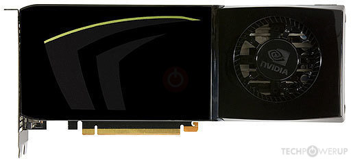
Being a dual-slot card, the NVIDIA GeForce GTX 285 draws power from 2x 6-pin power connectors, with power draw rated at 204 W maximum. Display outputs include: 2x DVI, 1x S-Video. GeForce GTX 285 is connected to the rest of the system using a PCI-Express 2.0 x16 interface. The card measures 267 mm in length, and features a dual-slot cooling solution. Its price at launch was 359 US Dollars.
Being a dual-slot card, the NVIDIA GeForce GTX 285 draws power from 2x 6-pin power connectors, with power draw rated at 204 W maximum. Display outputs include: 2x DVI, 1x S-Video. GeForce GTX 285 is connected to the rest of the system using a PCI-Express 2.0 x16 interface. The card measures 267 mm in length, and features a dual-slot cooling solution. Its price at launch was 359 US Dollars.
Graphics Processor
Graphics Card
- Release Date
- Dec 23rd, 2008
- Availability
- Jan 15th, 2009
- Generation
- GeForce 200
- Predecessor
- GeForce 9
- Successor
- GeForce 400
- Production
- End-of-life
- Launch Price
- 359 USD
- Bus Interface
- PCIe 2.0 x16
- Reviews
- 88 in our database
Relative Performance
Based on TPU review data: "Performance Summary" at 1920x1080, 4K for RTX 3080 and faster.
Clock Speeds
- GPU Clock
- 648 MHz
- Shader Clock
- 1476 MHz
- Memory Clock
-
1242 MHz
2.5 Gbps effective
Memory
- Memory Size
- 1024 MB
- Memory Type
- GDDR3
- Memory Bus
- 512 bit
- Bandwidth
- 159.0 GB/s
Render Config
- Shading Units
- 240
- TMUs
- 80
- ROPs
- 32
- SM Count
- 30
- L2 Cache
- 256 KB
Theoretical Performance
- Pixel Rate
- 20.74 GPixel/s
- Texture Rate
- 51.84 GTexel/s
- FP32 (float)
- 708.5 GFLOPS
- FP64 (double)
- 88.56 GFLOPS (1:8)
Board Design
- Slot Width
- Dual-slot
- Length
- 267 mm
10.5 inches
- TDP
- 204 W
- Suggested PSU
- 550 W
- Outputs
- 2x DVI
1x S-Video
- Power Connectors
- 2x 6-pin
- Board Number
- P891 SKU 52,
P892 SKU 52,
P892 SKU 55
Graphics Features
- DirectX
- 11.1 (10_0)
- OpenGL
- 3.3
- OpenCL
- 1.1
- Vulkan
- N/A
- CUDA
- 1.3
- Shader Model
- 4.0
GT200B GPU Notes
| PureVideo HD: VP2 VDPAU: Feature Set A GT200B, commonly printed on the chip package as G200-xxx-Bx is an optical shrink of the G200 core to the newer 55 manufacturing process of TSMC. It helped shrink the core's energy and thermal footprints to a level that even facilitated building a dual-GPU accelerator Latest Drivers: Windows 2000: Quadro Release 261.19 Windows XP / Server 2003 x64: GeForce Release 185.81 (Notebooks) GeForce Release 340.52 Quadro Release R319 U2 (321.01) Tesla Release 258.96 Windows Vista: GeForce Release 307.83 (Notebooks) GeForce Release 342.01 Quadro Release R340 U15 (342.01) Tesla Release 258.96 Windows 7 / 8 / 8.1 / 10: GeForce Release 342.01 Quadro Release R340 U15 (342.01) Tesla Release 258.96 |
Retail boards based on this design (20)
| Name | GPU Clock | Memory Clock | Other Changes |
|---|---|---|---|
| 670 MHz | 1300 MHz | ||
| 712 MHz | 1380 MHz | ||
| 662 MHz | 1242 MHz | ||
| 648 MHz | 1242 MHz | 2x DVI 1x HDMI | |
| 648 MHz | 1161 MHz | 2 GB | |
| 675 MHz | 1269 MHz | 2x DVI | |
| 720 MHz | 1390 MHz | ||
| 702 MHz | 1224 MHz | 2 GB | |
| 720 MHz | 1390 MHz | ||
| 675 MHz | 1188 MHz | 2 GB | |
| 702 MHz | 1323 MHz | ||
| 702 MHz | 1323 MHz | ||
| 675 MHz | 1269 MHz | ||
| 675 MHz | 1269 MHz | ||
| 648 MHz | 1242 MHz | ||
| 680 MHz | 1280 MHz | 270 mm/10.6 inches | |
| 680 MHz | 1280 MHz | 270 mm/10.6 inches, 1x DVI 1x HDMI 1x VGA | |
| 680 MHz | 1242 MHz | 2 GB | |
| 702 MHz | 1296 MHz | ||
| 722 MHz | 1350 MHz |


Jul 28th, 2025 18:23 CDT
change timezone
Latest GPU Drivers
New Forum Posts
- Inno3D iChiLL (1)
- Which Linux flavor? (76)
- What are you playing? (24022)
- Spoiler Alert........this car is fast. (254)
- Warning about DOCP (22)
- Kindly help me to complete my new PC build... (18)
- What's your latest tech purchase? (24382)
- Future-Proof Build for Music Production and Work - Will these parts work well together? (18)
- What antivirus do you use? (35)
- 2022-X58/1366 PIN Motherboards NVME M.2 SSD BIOS MOD Collection (947)
Popular Reviews
- Herman Miller Logitech G Embody Review - No Pain, No Gain
- Lian Li O11 Dynamic Mini V2 Review
- AQIRYS Sirius Pro Review
- Noctua NF-A12x25 G2 PWM Fan Review
- Upcoming Hardware Launches 2025 (Updated May 2025)
- VAXEE XE V2 Wireless Review
- UPERFECT UMax 24 Review
- DDR5 Memory Performance Scaling with AMD Zen 5
- Sharkoon OfficePal C10 Review - Affordable and Decent
- AMD Ryzen 7 9800X3D Review - The Best Gaming Processor
TPU on YouTube
Controversial News Posts
- AMD's Upcoming UDNA / RDNA 5 GPU Could Feature 96 CUs and 384-bit Memory Bus (134)
- AMD Radeon RX 9070 XT Gains 9% Performance at 1440p with Latest Driver, Beats RTX 5070 Ti (131)
- NVIDIA GeForce RTX 5080 SUPER Could Feature 24 GB Memory, Increased Power Limits (115)
- Intel "Nova Lake-S" Core Ultra 3, Ultra 5, Ultra 7, and Ultra 9 Core Configurations Surface (108)
- NVIDIA DLSS Transformer Cuts VRAM Usage by 20% (100)
- DDR6 Memory Arrives in 2027 with 8,800-17,600 MT/s Speeds (99)
- AMD Sampling Next-Gen Ryzen Desktop "Medusa Ridge," Sees Incremental IPC Upgrade, New cIOD (97)
- Intel CEO Confirms SMT To Return to Future CPUs (95)