Report an Error


AMD Xbox One S GPU
- Graphics Processor
- Durango 2
- Cores
- 768
- TMUs
- 48
- ROPs
- 16
- Memory Size
- 8 GB
- Memory Type
- DDR3
- Bus Width
- 256 bit
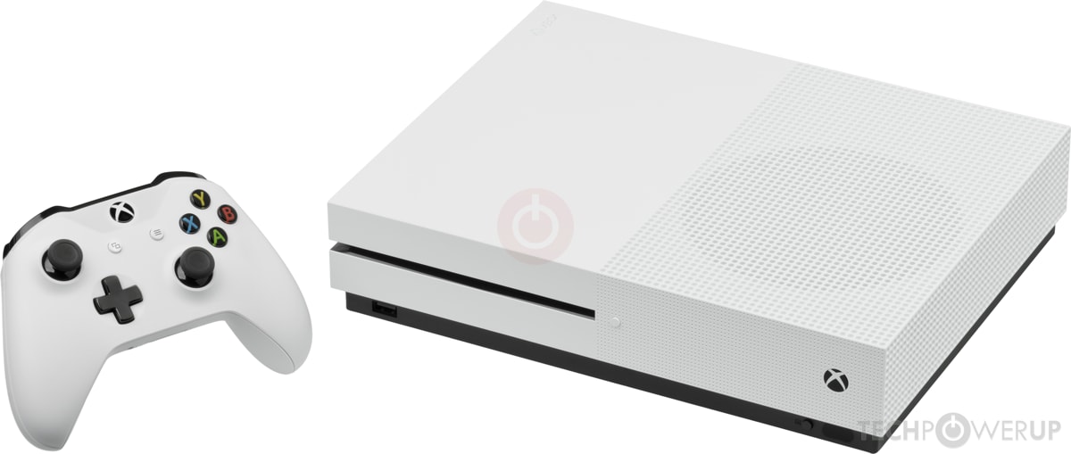

GPU
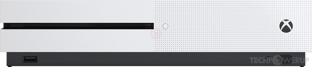
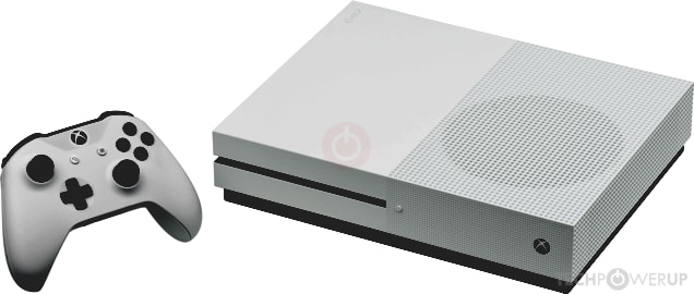
Front 2
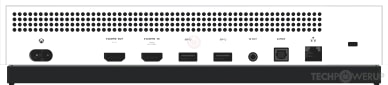
Back
Recommended Gaming Resolutions:
- 1280x720
- 1366x768
- 1600x900
The Xbox One S GPU was a high-end gaming console graphics solution by AMD, launched on August 2nd, 2016. Built on the 16 nm process, and based on the Durango 2 graphics processor, in its M1004145-001 variant, the device supports DirectX 12. The Durango 2 graphics processor is an average sized chip with a die area of 240 mm² and 5,000 million transistors. It features 768 shading units, 48 texture mapping units, and 16 ROPs. AMD includes 8 GB DDR3 memory, which are connected using a 256-bit memory interface. The GPU is operating at a frequency of 914 MHz, memory is running at 1066 MHz.
Its power draw is rated at 95 W maximum. The console's dimensions are 295 mm x 230 mm x 64 mm, and it features a igp cooling solution. Its price at launch was 399 US Dollars.
Its power draw is rated at 95 W maximum. The console's dimensions are 295 mm x 230 mm x 64 mm, and it features a igp cooling solution. Its price at launch was 399 US Dollars.
Graphics Processor
Graphics Card
- Release Date
- Aug 2nd, 2016
- Generation
-
Console GPU
(Microsoft)
- Production
- End-of-life
- Launch Price
- 399 USD
Clock Speeds
- GPU Clock
- 914 MHz
- Memory Clock
-
1066 MHz
2.1 Gbps effective
Memory
- Memory Size
- 8 GB
- Memory Type
- DDR3
- Memory Bus
- 256 bit
- Bandwidth
- 68.22 GB/s
Render Config
- Shading Units
- 768
- TMUs
- 48
- ROPs
- 16
- Compute Units
- 12
Theoretical Performance
- Pixel Rate
- 14.62 GPixel/s
- Texture Rate
- 43.87 GTexel/s
- FP32 (float)
- 1,403.9 GFLOPS
Board Design
- Length
- 295 mm
11.6 inches
- Width
- 230 mm
9.1 inches
- Height
- 64 mm
2.5 inches
- Weight
- 2.9 kg (6.4 lbs)
- Storage
- 1 TB HDD
- TDP
- 95 W
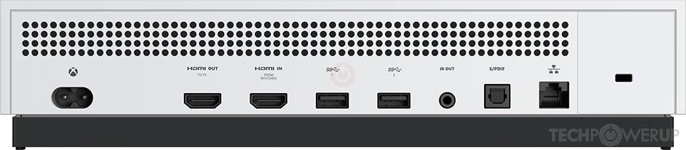
- Outputs
- 1x HDMI 2.0a
- Inputs
- 1x HDMI 1.4b
Graphics Features
- DirectX
- 12 (11_1)
- OpenGL
- N/A
- OpenCL
- 1.2
- Vulkan
- 1.1
- Shader Model
- 5.1
Durango 2 GPU Notes
| Generation: Sea Islands Codename: Gladius / Bishop CLRX: GCN 1.0 Instruction issue rate: 12 SCs * 4 SIMDs * 16 threads/clock = 768 ops/clock FLOPs: 768 ops/clock * (1 mul + 1 add) * 914 MHz = 1.404 TFLOPS Interpolation: (768 ops/clock / 2 ops) * 914 MHz = 350.97 Gfloat/sec Triangle rate: 2 tri/clock * 914 MHz = 1.828 Gtri/sec Vertex rate: 2 vert/clock * 914 MHz = 1.828 Gvert/sec Vertex/buffer fetch rate: (4 bytes) 4 elements/clock * 12 SCs * 914 MHz = 43.872 Gelement/sec Vertex/Buffer data rate from cache: 43.872 Gelements/sec * 4 bytes = 175.488 GB/sec Peak throughput from main RAM: 68.2 GB/sec Peak throughput from ESRAM: 128 bytes/clock * 914 MHz = 116.992 GB/sec ESRAM size: 32 MB GSM size: 64 KB LSM size: 12 SCs * 64 KB = 768 KB L2 cache size: 4 x 128 KB = 512 KB (shared) Bilinear fetch rate: (4 bytes) 4 fetches/clock * 12 SCs * 914 MHz = 43.872 Gtexels/sec Bilinear data rate from cache: 43.872 Gtexels/sec * 4 bytes = 175.488 GB/sec L1 cache size: 16 KB/SC * 12 SCs = 192 KB (nonshared) Pixel clear rate: 1 8×8 tile/clock * 4 DBs * 914 MHz = 233.984 Gpixel/sec Pixel hierarchical Z Rate: 1 8×8 tile/clock * 4 DBs * 914 MHz = 233.984 Gpixel/sec Sample Z rate: 16 /clock * 4 DBs * 914 MHz = 58.496 Gsample/sec Pixel rate: 4 /clock * 4 DBs * 914 MHz = 14.624 Gpixel/sec |
Aug 2nd, 2025 03:01 CDT
change timezone
Latest GPU Drivers
New Forum Posts
- What's your latest tech purchase? (24429)
- Free Games Thread (4838)
- 3DMARK "LEGENDARY" (359)
- memory used for store firmware in adapters wifi usb (4)
- Samsung 870 EVO - Beware, certain batches prone to failure! (1306)
- What antivirus do you use? (61)
- Laptop WWAN SSD? (4)
- I just bought an RX570 4Gb (27)
- TechPowerUp Screenshot Thread (MASSIVE 56K WARNING) (4285)
- Question about Intel Optane SSDs (90)
Popular Reviews
- ASUS ROG Crosshair X870E Apex Review
- MSI Claw 8 AI+ A2VM Review
- Montech X5 Review
- Orbital Pathfinder Review
- Herman Miller Logitech G Embody Review - No Pain, No Gain
- Lenovo Legion 5i (15IRX10) Review - Feature-Rich and Wallet Friendly
- Lian Li HydroShift II LCD-C 360TL Review
- Upcoming Hardware Launches 2025 (Updated May 2025)
- Noctua NF-A12x25 G2 PWM Fan Review
- Lian Li O11 Dynamic Mini V2 Review
TPU on YouTube
Controversial News Posts
- AMD's Upcoming UDNA / RDNA 5 GPU Could Feature 96 CUs and 384-bit Memory Bus (138)
- AMD Radeon RX 9070 XT Gains 9% Performance at 1440p with Latest Driver, Beats RTX 5070 Ti (131)
- Intel "Nova Lake-S" Core Ultra 3, Ultra 5, Ultra 7, and Ultra 9 Core Configurations Surface (110)
- DDR6 Memory Arrives in 2027 with 8,800-17,600 MT/s Speeds (102)
- NVIDIA to Debut GeForce RTX 50-series SUPER GPUs by Christmas (101)
- AMD Sampling Next-Gen Ryzen Desktop "Medusa Ridge," Sees Incremental IPC Upgrade, New cIOD (97)
- Intel CEO Confirms SMT To Return to Future CPUs (95)
- NVIDIA Becomes First Company Ever to Hit $4 Trillion Market-Cap (94)